
Решил написать о современных технологиях памяти. Желание появилось сразу после того, как я понял, что ни черта не разбираюсь в том, какая память какая и когда ее нужно ставить и куда вообще.
Начнем без особых вступлений, ибо памятей много, а времени мало.
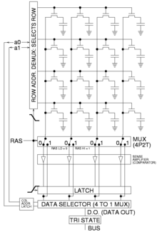
Итак, наиболее часто память с произвольным доступом(более известна как RAM) представляется в виде матрицы.

Тут все просто. Если мы хотим прочитать или записать что-то по определенному адресу, то мы передаем этот самый адрес, шевелим нужными пинами и на выходе получаем данные (ну или подаем данные, если вы больше предпочитаете записывать). В память как правило встроены декодеры адреса, которые по заданному адресу выбирают определенную колонку или столбец (об этом будет дальше).
Для начала перечислим основные параметры памяти, на которые ориентируются производители.
Во-первых, память должна предоставлять быстрый доступ к определенным своим битам.
Во-вторых, память должна достаточно быстро отвечать процессору (параметр, называемый latency).
В-третьих, память должна быть дешевой (ага, конечно).
В-четвертых, память должна потреблять мало энергии.
В-пятых, память должна быть предназначена для работы на определенном уровне в иерархии. Здесь имеется в виду тот факт, что, чем ближе к процессору находится память (не физически, хотя и это тоже), тем быстрее она должна работать.
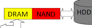
Забегая вперед, рассмотрим архитектуру типичного компьютера с точки зрения памяти.

Как правило, NOR-память содержит команды инициализации процессора. На это есть свои причины, которые мы рассмотрим позже. Обычно мы работаем с жестким диском. Процессор не может напрямую с ним работать, ему нужна некоторая помощь. В памяти NOR хранится управляющая процессором программа, которая, говорит ему, что делать дальше. Память NOR энергонезависима и довольно быстра (среди энергонезависимых), поэтому программу инициализации процессора лучше всего хранить в NOR-памяти. Однако в качестве буфера она использоваться вряд ли может. Самая главная причина заключается в том, что отношение стоимости памяти к ее размеру крайне велико. Да и скорость ее не так велика по сравнению с DRAM.
Можно заметить маленький зеленый квадратик на жестком диске. Тут тоже все просто. Жесткий диск — тоже устройство и имеет право иметь собственный контроллер, который тоже надо инициализировать.
С видеоадаптером ситуация аналогична. Можно отметить, что иногда у него DRAM не совсем собственная, а разделена с DRAM CPU.
Еще один тип памяти не отмечен на схеме. Этот тип EEPROM. Это крайне медленная дешевая энергонезависимая память, предназначенная специально для хранения серийников и прочего хлама.
А теперь небольшое дополнение к схеме, которое позволит системе работать быстрее.
Это дополнение — так называемый дисковый кэш. Он позволяет значительно ускорить доступ к информации на жестком диске (а заодно и выполнить пятое условие для памяти — это тот, что про иерархию памяти в системах).
На самом деле NAND память не общается напрямую с DRAM, и жесткий диск не пишет напрямую в NAND. Все это кроется за довольно сложными схемами. Но с точки зрения потоков информации нам этого вполне достаточно.
Теперь рассмотрим, как дела обстоят с серверами.
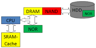
Здесь добавляется кэш процессора. Он необходима для очень быстрого доступа к данным. Мы знаем, что у процессора уже имеются собственные кэши (L1 и L2). Они по своей сути тоже являются SRAM-памятью.
Теперь посмотрим, что внутри плееров и камер.

В ROM хранится прошивка, которую можно менять (поэтому она не совсем ROM и может быть NOR). SRAM здесь нужна в качестве площадки для «памятезатратных» операций процессора. Таковыми являются кодирование видео и звука или изображений. Основным элементом является NAND память. Она выбрана из-за того что она энергонезависимая, быстрая для целей устройства и относительно недорогая.
Ну а теперь подробно про каждый тип.
Начнем с SRAM.
Каждый бит памяти является триггером и состоит из четырех транзисторов (в случае активной подтяжки линий) или из двух транзисторов и двух резисторов (в случае пассивной подтяжки линий). Как мы помним, память выстроена в линии. В случае SRAM это тоже так, и для каждой линии необходимо еще два транзистора. Для вывода информации SRAM использует дифференциальные линии. А как известно, дифференциальные линии крайне устойчивы к помехам. И как следствие, SRAM крайне быстра.

Нижняя пара транзисторов образует триггер с перекрестными обратными связями (cross-coupled flip-flop). Верхние транзисторы выполняют роль активной подтяжки. Транзисторы по бокам выставляют на прямой и инвертированной линии битов значения, хранящиеся в триггере при подаче сигнала на линию слов.
Для чтения подаем на Word line единицу и смотрим, что на bit line. Для записи зануляем необходимую bit line и подаем на word line единицу. Но это неинтересно.
Сильными сторонами этого типа памяти являются ее высокая скорость (благодаря применению дифференциальных линий и самой методики хранения) и низкое потребление в режиме неактивности (энергия потребляется только для изменения состояния триггера).
А вот слабыми сторонами является крайняя дороговизна памяти (6 или 4 транзистора на один бит — это много).
Перейдем к DRAM.
Здесь каждый бит представлен конденсатором и транзистором. Это значительно сокращает стоимость памяти по сравнению с SRAM.
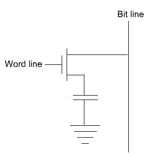
Как следствие наличия токов утечки кондесатора, DRAM память необходимо периодически обновлять (подзаряжать). Сама подзарядка является сложным процессом. Необходимо выбрать время сканирования битов и вкачивать заряд только туда, где была (или остается) единица. На самом деле схема оказывается еще сложнее, и как она устроена точно знают только производители памяти. Да и неважно это, как внутри происходит поддержание состояний битов, а важно следствие из этого факта. А следствие такое: на все это расходуется энергия, причем довольно большая.
Чтение и запись производится открытием и закрытием транзистора. Чтобы записать значение, нужно закрыть транзистор, и выставить потенциал на линии битов. Сопротивление сток-исток стремится к бесконечности, и конденсатор зарядится (разрядится). Для чтения нужно открыть транзистор и посмотреть, что на линии битов. После чтения необходимо провести принудительную процедуру обновления состояния бита (мы же не просто так получаем инфу о состоянии бита, а путем слития с конденсатора заряда). Эта процедура опять добавляет расход энергии.
Преимуществами DRAM являются ее дешевизна и скорость (здесь не сравниваем с SRAM).
Недостатками будут ее энергозависимость, необходимость обновления и высокое энергопотребление.
А теперь перейдем к энергонезависмым типам.
Самой первой разработанной и применяемой энергонезависимой памятью являлась mask ROM. Каждый бит в ней состоял только из транзистора.

Она очень похожа на DRAM, только в ней нет конденсатора. Mask ROM программируется преимущественно на фабрике и больше не может быть изменена. Само программирование производится путем металлизации одного из контактактов транзистора. Скажем, убираем у транзистора затвор (пережигается «проволочка» на схеме). И в результате на линии битов мы не сможем наблюдать 0.
Стоит еще раз отметить, что такая память изготавливается на фабриках. Это значит, что ее производство будет происходить только в крупных сериях, при которых окупятся затраты на изготовление масок и прочую подготовку микросхем к производству.
Преимуществами Mask ROM являются ее энергонезависимость, произвольный доступ, и дешевизна (при больших партиях).
Недостатками являются ее одноразовость и возможность программирования только на фабрике.
Однако люди хотят сохранять свои изображения, музыку в память, стирать все это и чувствовать себя абсолютно независимыми. На помощь пришло изобретение, называемое «плавающий затвор», разработанное в BellLabs задолго до того, как люди стали думать о необходимости энергонезависимой памяти.
Эх! Какая же это классная компания, где было разработано почти все, что мы сейчас знаем, где трудилось множество Нобелевских лауреатов… И почему она распалась, а остались теперь только патентные говнари… Ну да ладно…
Посмотрим, что это за зверь, плавающий затвор.
В таком типе памяти каждый бит представлен транзистором, который сохраняет заряд при отключении питания.

На картинке желтым показаны слои оксида, голубым — полупроводник и зеленым — подложка (тоже полупроводник, но не такой важный).
Электроны движутся от истока к затвору по каналу (в упрощенной форме). Сам плавающий затвор скрывается между слоями оксида. Нижний слой оксида называется слоем туннелирования, а верхний слой — слоем изоляции затвора. Я мог напутать с терминами, но так как я основываюсь на английской литературе, то перевожу так, как написано там. В отечественных источниках я не встречал четкого выделения названий этих слоев.
Рассмотрим первый эффект ,который применяется в плавающем затворе — инжекция горячих электронов.

Пусть по каналу течет большой ток, а на затвор наведен положительный потенциал. Тогда электроны с высокой кинетической энергией будут способны преодолеть барьер и осесть в плавающем затворе. Так происходит запись памяти.
Теперь рассмотрим эффект Фаулера-Нордхейма. Это по сути туннелирование электронов за счет изменения потенциала между затвором и истоком.

В результате в области истока образуется канал туннелирования, по которому заряд стекает с плавающего затвора.
Считается, что туннельный эффект Фаулера-Нордхейма крайне медленный процесс по сравнению с инжекцией горячих электронов. Но с помощью него мы можем как записывать, так и стирать память (просто поменяем плюс с минусом на затворе и истоке).
Есть у плавающего затвора серьезный недостаток.
Дело в том, что оксид это структура, в которой наличествует множество дефектов кристаллической решетки. Эти дефекты называются ловушками. в этих ловушках могут оседать электроны, так и не туннелировавшись в плавающий затвор. Все эти электроны могут проявляться как ложный накопившийся заряд. И теперь становится понятно, почему количество циклов перезаписи ограничено. Все потому что электроны в ловушках все копятся и копятся с каждым циклом.
В большинстве случаев ограниченное количество циклов не является проблемой. Их хоть конечное число, но их много. Для SLC NAND их порядка 500 000, а для MLC NAND их десятки тысяч.
Теперь перейдем к конкретным типам памяти.
EEPROM.
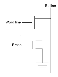
Ячейка EEPROM состоит из двух транзисторов: один с плавающим затвором и еще транзистор для снятия данных. Стирание данных производится непосредственно подачей потенциала на затвор транзистора памяти, а чтение — на транзистор снятия данных.
EEPROM очень медленная память, потому что использует механизм туннелирования.
Особенностью Flash памяти является использование одного транзистора для стирания группы битов. Эта идея является неким компромисом между стоимостью памяти и удобством ее использования.
Начнем обзор Flash памяти с NOR.

NOR-память организована как двумерный массив. Доступ к ячейке может производиться индивидуально и быстро. Чтение производится включением потенциала на линии затворов и чтением тока стока.
Преимуществами NOR являются быстрый произвольный доступ в любой момент времени к любой ячейке. Сама ячейка состоит из одного транзистора, что удешевляет память.
Недостатками являются медленные записи.
В NAND Flash нашли способ еще уменьшить размер чипа. Для этого сократили количество линий истоков. Чип памяти уже не имел свойства произвольного доступа к каждой ячейке, но зато значительно сокращался в размере. На изображении представлена одна строка в NAND-памяти.

Помимо потери произвольного доступа появилась еще одна проблема. Дело в том, что чем меньше количество линий в чипе, тем они длиннее, а чем они длиннее, тем больше шумов. Так что в NAND велика вероятность словить ошибку чтения. Чтобы устранить этот недостаток применяется помехоустойчивое кодирование информации. После блока памяти оставляется несколько бит для ECC — error correction code. Он является неким хэшем от данных, записанных в блоке. Для имплементации этой защиты требуется довольно сложная логика, которая будет контролировать потоки данных.
Итак, после того как были описаны все распространенные типы памяти, самое время свести их в итоговую таблицу.
Начнем с оперативных энергозависимых. Заголовки в таблице я не переводил, потому что русский перевод не влез бы и звучал бы он дебильно (но все же перевод вот: минимальный размер данных на запись, минимальный размер данных на чтение, скорость записи, скорость чтения, энергопотребление в активной фазе, энергопотребление в режиме ожидания, цена за мегабайт, приложения).
| Smallest Write | Smallest Read | Write Speed | Read Speed | Active Power | Sleep Power | Price | Applications | |
| SRAM | Байт | Байт | Очень быстро | Очень быстро | Высокое | Очень низкое | Очень высокая | Мало быстрой памяти |
| DRAM | Байт | Страница | Быстро | Быстро | Среднее | Высокое | Низкая | Основное ОЗУ |
А теперь такая же таблица для энергозависимой памяти.
From Wikipedia, the free encyclopedia

Layout for the silicon implementation of a six transistor SRAM memory cell.
The memory cell is the fundamental building block of computer memory. The memory cell is an electronic circuit that stores one bit of binary information and it must be set to store a logic 1 (high voltage level) and reset to store a logic 0 (low voltage level). Its value is maintained/stored until it is changed by the set/reset process. The value in the memory cell can be accessed by reading it.
Over the history of computing, different memory cell architectures have been used, including core memory and bubble memory. Today, the most common memory cell architecture is MOS memory, which consists of metal–oxide–semiconductor (MOS) memory cells. Modern random-access memory (RAM) uses MOS field-effect transistors (MOSFETs) as flip-flops, along with MOS capacitors for certain types of RAM.
The SRAM (static RAM) memory cell is a type of flip-flop circuit, typically implemented using MOSFETs. These require very low power to keep the stored value when not being accessed. A second type, DRAM (dynamic RAM), is based around MOS capacitors. Charging and discharging a capacitor can store a ‘1’ or a ‘0’ in the cell. However, the charge in this capacitor will slowly leak away, and must be refreshed periodically. Because of this refresh process, DRAM uses more power. However, DRAM can achieve greater storage densities.
On the other hand, most non-volatile memory (NVM) is based on floating-gate memory cell architectures. Non-volatile memory technologies including EPROM, EEPROM and flash memory use floating-gate memory cells, which are based around floating-gate MOSFET transistors.
Description[edit]
The memory cell is the fundamental building block of memory. It can be implemented using different technologies, such as bipolar, MOS, and other semiconductor devices. It can also be built from magnetic material such as ferrite cores or magnetic bubbles.[1] Regardless of the implementation technology used, the purpose of the binary memory cell is always the same. It stores one bit of binary information that can be accessed by reading the cell and it must be set to store a 1 and reset to store a 0.[2]
Significance[edit]
Square array of DRAM memory cells being read
Logic circuits without memory cells are called combinational, meaning the output depends only on the present input.
But memory is a key element of digital systems. In computers, it allows to store both programs and data and memory cells are also used for temporary storage of the output of combinational circuits to be used later by digital systems.
Logic circuits that use memory cells are called sequential circuits, meaning the output depends not only on the present input, but also on the history of past inputs.
This dependence on the history of past inputs makes these circuits stateful and it is the memory cells that store this state.
These circuits require a timing generator or clock for their operation.[3]
Computer memory used in most contemporary computer systems is built mainly out of DRAM cells; since the layout is much smaller than SRAM, it can be more densely packed yielding cheaper memory with greater capacity. Since the DRAM memory cell stores its value as the charge of a capacitor, and there are current leakage issues, its value must be constantly rewritten. This is one of the reasons that make DRAM cells slower than the larger SRAM (static RAM) cells, which has its value always available. That is the reason why SRAM memory is used for on-chip cache included in modern microprocessor chips.[4]
History[edit]

On December 11, 1946 Freddie Williams applied for a patent on his cathode-ray tube (CRT) storing device (Williams tube) with 128 40-bit words. It was operational in 1947 and is considered the first practical implementation of random-access memory (RAM).[5] In that year, the first patent applications for magnetic-core memory were filed by Frederick Viehe.[6][7] Practical magnetic-core memory was developed by An Wang in 1948, and improved by Jay Forrester and Jan A. Rajchman in the early 1950s, before being commercialised with the Whirlwind computer in 1953.[8] Ken Olsen also contributed to its development.[9]
Semiconductor memory began in the early 1960s with bipolar memory cells, made of bipolar transistors. While it improved performance, it could not compete with the lower price of magnetic-core memory.[10]
MOS memory cells[edit]

The invention of the MOSFET (metal–oxide–semiconductor field-effect transistor), also known as the MOS transistor, by Mohamed M. Atalla and Dawon Kahng at Bell Labs in 1959,[11] enabled the practical use of metal–oxide–semiconductor (MOS) transistors as memory cell storage elements, a function previously served by magnetic cores.[12] The first modern memory cells were introduced in 1964, when John Schmidt designed the first 64-bit p-channel MOS (PMOS) static random-access memory (SRAM).[13][14]
SRAM typically has six-transistor cells, whereas DRAM (dynamic random-access memory) typically has single-transistor cells.[15][13] In 1965, Toshiba’s Toscal BC-1411 electronic calculator used a form of capacitive bipolar DRAM, storing 180-bit data on discrete memory cells, consisting of germanium bipolar transistors and capacitors.[16][17] MOS technology is the basis for modern DRAM. In 1966, Dr. Robert H. Dennard at the IBM Thomas J. Watson Research Center was working on MOS memory. While examining the characteristics of MOS technology, he found it was capable of building capacitors, and that storing a charge or no charge on the MOS capacitor could represent the 1 and 0 of a bit, while the MOS transistor could control writing the charge to the capacitor. This led to his development of a single-transistor DRAM memory cell.[18] In 1967, Dennard filed a patent for a single-transistor DRAM memory cell, based on MOS technology.[19]
The first commercial bipolar 64-bit SRAM was released by Intel in 1969 with the 3101 Schottky TTL. One year later, it released the first DRAM integrated circuit chip, the Intel 1103, based on MOS technology. By 1972, it beat previous records in semiconductor memory sales.[20] DRAM chips during the early 1970s had three-transistor cells, before single-transistor cells became standard since the mid-1970s.[15][13]
CMOS memory was commercialized by RCA, which launched a 288-bit CMOS SRAM memory chip in 1968.[21] CMOS memory was initially slower than NMOS memory, which was more widely used by computers in the 1970s.[22] In 1978, Hitachi introduced the twin-well CMOS process, with its HM6147 (4 kb SRAM) memory chip, manufactured with a 3 µm process. The HM6147 chip was able to match the performance of the fastest NMOS memory chip at the time, while the HM6147 also consumed significantly less power. With comparable performance and much less power consumption, the twin-well CMOS process eventually overtook NMOS as the most common semiconductor manufacturing process for computer memory in the 1980s.[22]
The two most common types of DRAM memory cells since the 1980s have been trench-capacitor cells and stacked-capacitor cells.[23] Trench-capacitor cells are where holes (trenches) are made in a silicon substrate, whose side walls are used as a memory cell, whereas
stacked-capacitor cells are the earliest form of three-dimensional memory (3D memory), where memory cells are stacked vertically in a three-dimensional cell structure.[24] Both debuted in 1984, when Hitachi introduced trench-capacitor memory and Fujitsu introduced stacked-capacitor memory.[23]
Floating-gate MOS memory cells[edit]
The floating-gate MOSFET (FGMOS) was invented by Dawon Kahng and Simon Sze at Bell Labs in 1967.[25] They proposed the concept of floating-gate memory cells, using FGMOS transistors, which could be used to produce reprogrammable ROM (read-only memory).[26] Floating-gate memory cells later became the basis for non-volatile memory (NVM) technologies including EPROM (erasable programmable ROM), EEPROM (electrically erasable programmable ROM) and flash memory.[27]
Flash memory was invented by Fujio Masuoka at Toshiba in 1980.[28][29] Masuoka and his colleagues presented the invention of NOR flash in 1984,[30] and then NAND flash in 1987.[31] Multi-level cell (MLC) flash memory was introduced by NEC, which demonstrated quad-level cells in a 64 Mb flash chip storing 2-bit per cell in 1996.[23] 3D V-NAND, where flash memory cells are stacked vertically using 3D charge trap flash (CTP) technology, was first announced by Toshiba in 2007,[32] and first commercially manufactured by Samsung Electronics in 2013.[33][34]
Implementation[edit]
The following schematics detail the three most used implementations for memory cells:
- The dynamic random access memory cell (DRAM);
- The static random access memory cell (SRAM);
- Flip-flops like the J/K shown below, using only logic gates.
|
DRAM cell (1 transistor and one capacitor). |
SRAM cell (6 transistors). |
|

Operation[edit]
DRAM memory cell[edit]
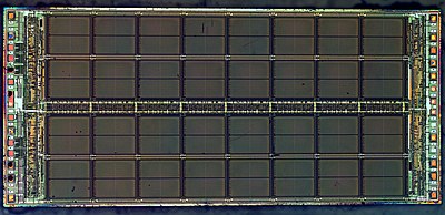
Die of the MT4C1024 (1994) integrating one-mebibit of DRAM memory cells.
Storage[edit]
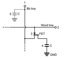
- The storage element of the DRAM memory cell is the capacitor labeled (4) in the diagram above. The charge stored in the capacitor degrades over time, so its value must be refreshed (read and rewritten) periodically. The nMOS transistor (3) acts as a gate to allow reading or writing when open or storing when closed.[35]
Reading[edit]
- For reading the Word line (2) drives a logic 1 (voltage high) into the gate of the nMOS transistor (3) which makes it conductive and the charge stored at the capacitor (4) is then transferred to the bit line (1). The bit line will have a parasitic capacitance (5) that will drain part of the charge and slow the reading process. The capacitance of the bit line will determine the needed size of the storage capacitor (4). It is a trade-off. If the storage capacitor is too small, the voltage of the bit line would take too much time to raise or not even rise above the threshold needed by the amplifiers at the end of the bit line. Since the reading process degrades the charge in the storage capacitor (4) its value is rewritten after each read.[36]
Writing[edit]
- The writing process is the easiest, the desired value logic 1 (high voltage) or logic 0 (low voltage) is driven into the bit line. The word line activates the nMOS transistor (3) connecting it to the storage capacitor (4). The only issue is to keep it open enough time to ensure that the capacitor is fully charged or discharged before turning off the nMOS transistor (3).[36]
SRAM memory cell[edit]

SRAM memory cell depicting Inverter Loop as gates

An animated SR latch. Black and white mean logical ‘1’ and ‘0’, respectively.
(A) S = 1, R = 0: set
(B) S = 0, R = 0: hold
(C) S = 0, R = 1: reset
(D) S = 1, R = 1: not allowed
Transitioning from the restricted combination (D) to (A) leads to an unstable state.
Storage[edit]
- The working principle of SRAM memory cell can be easier to understand if the transistors M1 through M4 are drawn as logic gates. That way it is clear that at its heart, the cell storage is built by using two cross-coupled inverters. This simple loop creates a bi-stable circuit. A logic 1 at the input of the first inverter turns into a 0 at its output, and it is fed into the second inverter which transforms that logic 0 back to a logic 1 feeding back the same value to the input of the first inverter. That creates a stable state that does not change over time. Similarly the other stable state of the circuit is to have a logic 0 at the input of the first inverter. After been inverted twice it will also feedback the same value.[37]
- Therefore there are only two stable states that the circuit can be in:
Reading[edit]
- To read the contents of the memory cell stored in the loop, the transistors M5 and M6 must be turned on. when they receive voltage to their gates from the word line (
 ), they become conductive and so the and values get transmitted to the bit line () and to its complement ().[37] Finally this values get amplified at the end of the bit lines.[37]


Writing[edit]
- The writing process is similar, the difference is that now the new value that will be stored in the memory cell is driven into the bit line () and the inverted one into its complement (). Next transistors M5 and M6 are open by driving a logic 1 (voltage high) into the word line (). This effectively connects the bit lines to the by-stable inverter loop. There are two possible cases:
- If the value of the loop is the same as the new value driven, there is no change;
- if the value of the loop is different from the new value driven there are two conflicting values, in order for the voltage in the bit lines to overwrite the output of the inverters, the size of the M5 and M6 transistors must be larger than that of the M1-M4 transistors. This allows more current to flow through first ones and therefore tips the voltage in the direction of the new value, at some point the loop will then amplify this intermediate value to full rail.[37]
Flip-flop[edit]
The flip-flop has many different implementations, its storage element is usually a latch consisting of a NAND gate loop or a NOR gate loop with additional gates used to implement clocking. Its value is always available for reading as an output. The value remains stored until it is changed through the set or reset process. Flip-flops are typically implemented using MOSFETs.
Floating gate[edit]

Floating-gate memory cells, based on floating-gate MOSFETs, are used for most non-volatile memory (NVM) technologies, including EPROM, EEPROM and flash memory.[27] According to R. Bez and A. Pirovano:
A floating-gate memory cell is basically an MOS transistor with a gate completely surrounded by dielectrics (Fig. 1.2), the floating-gate (FG), and electrically governed by a capacitive-coupled control-gate (CG). Being electrically isolated, the FG acts as the storing electrode for the cell device. Charge injected into the FG is maintained there, allowing modulation of the ‘apparent’ threshold voltage (i.e. VT seen from the CG) of the cell transistor.[27]
See also[edit]
- Dynamic random-access memory
- Flip-flop (electronics)
- Row hammer
- Static random-access memory
References[edit]
- ^ D. Tang, Denny; Lee, Yuan-Jen (2010). Magnetic memory: Fundamentals and technology. Cambridge University Press. p. 91. ISBN 978-1139484497. Retrieved 13 December 2015.
- ^ Fletcher, William (1980). An engineering approach to digital design. Prentice-Hall. p. 283. ISBN 0-13-277699-5.
- ^ Microelectronic circuits (Second ed.). Holt, Rinehart and Winston, Inc. 1987. p. 883. ISBN 0-03-007328-6.
- ^ «The technical question: the cache, how does it work?». PC World Fr (in French). Archived from the original on 30 March 2014.
- ^ O’Regan, Gerard (2013). Giants of computing: A compendium of select, pivotal pioneers. Springer. p. 267. ISBN 978-1447153405. Retrieved 13 December 2015.
- ^ Reilly, Edwin D. (2003). Milestones in computer science and information technology. Greenwood publishing group. p. 164. ISBN 9781573565219.
- ^ W. Pugh, Emerson; R. Johnson, Lyle; H. Palmer, John (1991). IBM’s 360 and early 370 systems. MIT Press. p. 706. ISBN 0262161230. Retrieved 9 December 2015.
- ^ «1953: Whirlwind computer debuts core memory». Computer History Museum. Retrieved 2 August 2019.
- ^ Taylor, Alan (18 June 1979). Computerworld: Mass. Town has become computer capital. IDG Enterprise. p. 25.
- ^ «1966: Semiconductor RAMs serve high-speed storage needs». Computer History Museum. Retrieved 19 June 2019.
- ^ «1960 — Metal oxide semiconductor (MOS) transistor demonstrated». The Silicon Engine. Computer history museum.
- ^ «Transistors — an overview». ScienceDirect. Retrieved 8 August 2019.
- ^ a b c «1970: Semiconductors compete with magnetic cores». Computer history museum. Retrieved 19 June 2019.
- ^ Solid state design — vol. 6. Horizon house. 1965.
- ^ a b «Late 1960s: Beginnings of MOS memory» (PDF). Semiconductor history museum of Japan. 23 January 2019. Retrieved 27 June 2019.
- ^ «Spec sheet for Toshiba «TOSCAL» BC-1411″. Old calculator web museum. Archived from the original on 3 July 2017. Retrieved 8 May 2018.
- ^ «Toshiba «Toscal» BC-1411 desktop calculator». Archived from the original on 20 May 2007.
- ^ «DRAM». IBM100. IBM. 9 August 2017. Retrieved 20 September 2019.
- ^ «Robert Dennard». Encyclopædia Britannica. Retrieved 8 July 2019.
- ^ Kent, Allen; Williams, James G. (6 January 1992). Encyclopedia of microcomputers: volume 9 — Icon programming language to knowledge-based systems: APL techniques. CRC press. p. 131. ISBN 9780824727086.
- ^ «1963: Complementary MOS circuit configuration is invented». Computer history museum. Retrieved 6 July 2019.
- ^ a b «1978: Double-well fast CMOS SRAM (Hitachi)» (PDF). Semiconductor history museum of Japan. Archived (PDF) from the original on 5 July 2019. Retrieved 5 July 2019.
- ^ a b c «Memory». Semiconductor technology online (STOL). Retrieved 25 June 2019.
- ^ «1980s: DRAM capacity increases, the shift to CMOS advances, and Japan dominates the market» (PDF). Semiconductor history museum of Japan. Retrieved 19 July 2019.
- ^ Kahng, D.; Sze, S.M. (1967). «A floating-gate and its application to memory devices». The Bell System Technical Journal. 46 (6): 1288–95. doi:10.1002/j.1538-7305.1967.tb01738.x.
- ^ «1971: Reusable semiconductor ROM introduced». Computer history museum. Retrieved 19 June 2019.
- ^ a b c Bez, R.; Pirovano, A. (2019). Advances in non-volatile memory and storage technology. Woodhead Publishing. ISBN 9780081025857.
- ^ Fulford, Benjamin (24 June 2002). «Unsung hero». Forbes. Archived from the original on 3 March 2008. Retrieved 18 March 2008.
- ^ US 4531203 Fujio Masuoka
- ^ «Toshiba: Inventor of flash memory». Toshiba. Archived from the original on 20 June 2019. Retrieved 20 June 2019.
- ^ Masuoka, F.; Momodomi, M.; Iwata, Y.; Shirota, R. (1987). «New ultra high density EPROM and flash EEPROM with NAND structure cell». Electron Devices Meeting, 1987 International. IEDM 1987. IEEE. doi:10.1109/IEDM.1987.191485.
- ^ «Toshiba announces new «3D» NAND flash technology». Engadget. 12 June 2007. Retrieved 10 July 2019.
- ^ «Samsung introduces world’s first 3D V-NAND based SSD for enterprise applications». Samsung semiconductor global website. Archived from the original on 15 April 2021.
- ^ Clarke, Peter (2013). «Samsung confirms 24 layers in 3D NAND». EE Times.
- ^ Jacob, Bruce; Ng, Spencer; Wang, David (28 July 2010). Memory systems: Cache, DRAM, disk. Morgan Kaufmann. p. 355. ISBN 9780080553849.
- ^ a b Siddiqi, Muzaffer A. (19 December 2012). Dynamic RAM: Technology advancements. CRC Press. p. 10. ISBN 9781439893739.
- ^ a b c d Li, Hai; Chen, Yiran (19 April 2016). Nonvolatile memory design: Magnetic, resistive, and phase change. CRC press. pp. 6, 7. ISBN 9781439807460.

В этой статье мы с Вами поговорим о том, что положено в основу создания и по какому принципу работает устройство флэш-памяти (не путайте с USB флэш-накопителями и картами памяти). Кроме этого, вы узнаете о ее преимуществах и недостатках перед другими типами ПЗУ (постоянно запоминающими устройствами) и познакомитесь с ассортиментом самых распространенных накопителей, которые содержат в себе флэш-память.
Основное достоинство этого устройства в том, что оно энергонезависимое и ему не нужно электричество для хранения данных. Всю хранящуюся информацию во флэш-памяти можно считать бесконечное количество раз, а вот количество полных циклов записи к сожалению ограничено.
Флэш-память (flash memory) — относится к полупроводникам электрически перепрограммируемой памяти (EEPROM). Благодаря техническим решениям, не высокой стоимости, большому объему, низкому энергопотреблению, высокой скорости работы, компактности и механической прочности, флэш-память встраивают в цифровые портативные устройства и носители информации.
У флэш-памяти перед другими накопителями (жесткие диски и оптические накопители) типа ПЗУ есть как свои преимущества, так и свои недостатки, с которыми вы можете познакомиться из таблицы расположенной ниже.
| Тип ПЗУ | Преимущества | Недостатки |
| Жесткий диск | Большой объем хранимой информации.
Высокая скорость работы. Дешевизна хранения данных (в расчете на 1 Мбайт). |
Большие габариты.
Чувствительность к вибрации. Тепловыделение. Шум. |
| Оптический диск | Удобство транспортировки.
Дешевизна хранения информации. Возможность тиражирования. |
Небольшой объем.
Нужно считывающее устройство. Ограничения при операциях (чтение, запись). Невысокая скорость работы. Чувствительность к вибрации. Шум. |
| Флэш-память | Высокая скорость доступа к данным.
Экономное энергопотребление. Устойчивость к вибрациям. Удобство подключения к компьютеру. Компактные размеры. |
Ограниченное количество циклов записи. |
Сегодня никто не сомневается в том, что флэш-память будет продолжать укреплять свои позиции в информационных технологиях, особенно в линейке мобильных устройств (КПК, планшеты, смартфоны, плееры). На основе флэш-памяти работают самые востребованные и популярные USB флэш-накопители и сменные карты памяти для электронных устройств (SD, MMC, miniSD…).
Карты памяти, как и USB накопители не стоят в стороне, а привлекают внимание потенциальных покупателей своим многообразием. От такого изобилия запоминающих устройств выигрывает только производитель, а потребитель испытывает ряд неудобств. Ведь всем нам знакомы такие ситуации, когда телефону нужна одна карта, КПК другая, фотоаппарату третья. Такой ассортимент накопителей на руку производителям, потому что они извлекают из широкой эксклюзивной продажи большую выгоду. Вот небольшой список распространенных накопителей с флэш-памятью:
- Compact Flash Type I (CF I)/Type II (CF II);
- Memory Styck (MS Pro, MS Duo);
- Secure Digital (SD);
- miniSD;
- xD-Picture Card (xD);
- MultiMedia Card (MMC).
- USB Flash Drive.
В одной из публикаций я писал о том как выбрать USB-флеш-накопитель, а о том как выбрать карту в формате SD (microSD, miniSD) читайте здесь.
Принцип работы флэш-памяти.
Элементарной ячейка хранения данных флэш-памяти представляет из себя транзистор с плавающим затвором. Особенность такого транзистора в том, что он умеет удерживать электроны (заряд). Вот на его основе и разработаны основные типы флэш-памяти NAND и NOR. Конкуренции между ними нет, потому что каждый из типов обладает своим преимуществом и недостатком. Кстати, на их основе строят гибридные версии такие как DiNOR и superAND.
Во флэш-памяти производители используют два типа ячеек памяти MLC и SLC.

- Флэш-память с MLC (Multi-level cell — многоуровневые ячейки памяти)ячейки более емкие и дешевые, но они с большим временем доступа и меньшим количеством циклов записи/стирания (около 10000).
- Флэш-память, которая содержит в себе SLC (Single-level cell — одноуровневые ячейки памяти) ячейки имеет максимальное количество циклов записи/стирания(100000) и обладают меньшим временем доступа.
Изменение заряда (запись/стирание) выполняется приложением между затвором и истоком большого потенциала, чтобы напряженность электрического поля в тонком диэлектрике между каналом транзистора и карманом оказалась достаточна для возникновения туннельного эффекта. Для усиления эффекта тунеллирования электронов в карман при записи применяется небольшое ускорение электронов путем пропускания тока через канал полевого транзистора.
Принцип работы флеш-памяти основан на изменении и регистрации электрического заряда в изолированной области («карман») полупроводниковой структуры.
Чтение выполняется полевым транзистором, для которого карман выполняет роль затвора. Потенциал плавающего затвора изменяет пороговые характеристики транзистора, что и регистрируется цепями чтения. Эта конструкция снабжается элементами, которые позволяют ей работать в большом массиве таких же ячеек.
Теперь рассмотрим более подробно ячейки памяти с одним и двумя транзисторами…
Ячейка памяти с одним транзистором.
Если на управляющий затвор подать положительное напряжения (инициализация ячейки памяти) то он будет находиться в открытом состоянии, что будет соответствовать логическому нулю.

А если на плавающий затвор поместить избыточный отрицательный заряд (электрон) и подать положительное напряжение на управляющий затвор ,то он компенсирует создаваемое управляющим затвором электрическое поле и не даст образовываться каналу проводимости, а значит транзистор будет находиться в закрытом состоянии.
Вот так, наличие или отсутствие заряда на плавающем затворе точно определяет состояние открыт или закрыт транзистор, когда подается одно и тоже положительное напряжения на управляющий затвор. Если мы будем рассматривать подачу напряжения на управляющий затвор, как инициализацию ячейки памяти, то по тому, какое напряжение между истоком и стоком можно судить о наличии или отсутствии заряда на плавающем затворе.
Таким образом получается своеобразная элементарная ячейка памяти, способная сохранять один информационный бит. Ко всему этому очень важно, чтобы заряд на плавающем затворе (если он там имеется) мог сохраняться там долго, как при инициализации ячейки памяти, так и при отсутствии напряжения на управляющем затворе. Только в этом случае ячейка памяти будет энергонезависимой.
Так каким же образом в случае необходимости на плавающий затвор помещать заряд (записывать содержимое ячейки памяти) и удалять его оттуда (стирать содержимое ячейки памяти) когда это необходимо.
Поместить заряд на плавающий затвор (процесс записи) можно методом инжекции горячих электронов (CHE-Channel Hot Electrons) или методом туннелирования Фаулера-Нордхейма.
Если используется метод инжекции горячих электронов, то на сток и управляющий затвор подается высокое напряжение, что придаст электронам в канале энергии, достаточной чтобы преодолеть потенциальный барьер, который создается тонким слоем диэлектрика, и направить (туннелировать) в область плавающего затвора (во время чтения на управляющий затвор подается меньшее напряжение и эффект туннелирования не происходит).

Чтобы удалить заряд с плавающего затвора (выполнить стирания ячейки памяти) на управляющий затвор подается высокое отрицательное напряжение (около 9 В), а на область истока подается положительное напряжение. Это приводит к тому, что электроны туннелируют из области плавающего затвора в область истока. Таким образом происходит квантовое туннелирование Фаулера — Нордхейма (Fowler — Nordheim).
Наверно вы уже поняли, что транзистор с плавающим затвором это элементарная ячейка флэш-памяти. Но ячейки с одним транзистором имеют некоторые недостатки, основным из которых является плохая масштабируемость.
Так как при создании массива памяти, каждая ячейка памяти (то есть транзистор) подключается к двум перпендикулярным шинам. Управляющие затворы подключаются к шине, которую называют линией слов (Word Line), а стоки соединяют с шиной, ее называют битовой линией (Bit Line). В следствии чего в схеме находится высокое напряжение и при записи методом инжекции горячих электронов все линии — слов, битов и истоков нужно разместить на большом расстоянии друг от друга. Это даст нужный уровень изоляции, но отразится на ограничении объема флэш-памяти.
Еще одним недостатком такой ячейки памяти является присутствие эффекта избыточного удаления заряда с плавающего затвора, а он не может компенсироваться процессом записи. В следствии этого на плавающем затворе образуется положительный заряд, что делает неизменным состояние транзистора и он всегда остается открытым.
Ячейка памяти с двумя транзисторами.
Двухтранзисторная ячейка памяти, это модифицированная однотранзисторная ячейка, в которой находится обычный КМОП-транзистор и транзистор с плавающим затвором. В этой структуре обычный транзистор выполняет роль изолятора транзистора с плавающим затвором от битовой линии.

Имеет ли преимущества двухтранзисторная ячейка памяти? Да, ведь с ее помощью можно создавать более компактные и хорошо масштабируемые микросхемы памяти, потому что здесь транзистор с плавающим затвором изолируется от битовой линии. Ко всему прочему, в отличии от однотранзисторной ячейки памяти, где информация записывается методом инжекции горячих электронов, в двухтранзисторной ячейки памяти для записи и стирания информации используется метод квантового туннелирования Фаулера — Нордхейма. Такой подход дает возможность снизить напряжение, которое необходимо для операции записи. Забегая наперед скажу, что двухтранзисторные ячейки применяются в памяти со структурой NAND.
Устройство флэш-памяти с архитектурой NOR.
Тип этой памяти является источником и неким толчком в развитии всей EEPROM. Ее архитектура была разработана компанией Intel в далеком 1988 году. Как было написано ранее, чтобы получить доступ к содержимому ячейки памяти (инициализировать ячейку), нужно подать напряжение на управляющий затвор.
Поэтому разработчики компании все управляющие затворы подсоединили к линии управления, которая называется линией слов (Word Line). Анализ информации ячейки памяти выполняется по уровню сигнала на стоке транзистора. Поэтому разработчики все стоки транзисторов подсоединили к линии, которая называется линией битов (Bit Line).

Архитектура NOR получила название благодаря логической операции ИЛИ — НЕ (в переводе с английского NOR). Принцип логической операции NOR заключается в том, что она над несколькими операндами (данные, аргумент операции…) дает единичное значение, когда все операнды равны нулю, и нулевое значение во всех остальных операциях.
В нашем случае под операндами подразумевается значение ячеек памяти, а значит в данной архитектуре единичное значение на битовой линии будет наблюдается только в том случае , когда значение всех ячеек, которые подключены к битовой линии, будут равны нулю (все транзисторы закрыты).
В этой архитектуре хорошо организован произвольный доступ к памяти, но процесс записи и стирания данных выполняется относительно медленно. В процессе записи и стирания применяется метод инжекции горячих электронов. Ко всему прочему микросхема флеш-памяти с архитектурой NOR и размер ее ячейки получается большим, поэтому эта память плохо масштабируется.

Флеш-память с архитектурой NOR как правило используют в устройствах для хранения программного кода. Это могут быть телефоны, КПК, BIOS системных плат…
Устройство флэш-памяти с архитектурой NAND.
Данный тип памяти был разработан компанией Toshiba. Эти микросхемы благодаря своей архитектуре применяют в маленьких накопителях , которые получили имя NAND (логическая операция И-НЕ). При выполнении операция NAND дает значение нуль только, когда все операнды равны нулю, и единичное значение во всех других случаях.
Как было написано ранее, нулевое значение это открытое состояние транзистора. В следствии этого в архитектуре NAND подразумевается, что битовая линия имеет нулевое значение в том случае, когда все подключенные к ней транзисторы открыты, и значение один, когда хотя бы один из транзисторов закрыт. Такую архитектуру можно построить, если подсоединить транзисторы с битовой линией не по одному (так построено в архитектуре NOR) , а последовательными сериями (столбец из последовательно включенных ячеек).

Данная архитектура по сравнению с NOR хорошо масштабируется потому, что разрешает компактно разместить транзисторы на схеме. Кроме этого архитектура NAND производит запись путем туннелирования Фаулера — Нордхейма, а это разрешает реализовать быструю запись нежели в структуре NOR. Чтобы увеличить скорость чтения, в микросхемы NAND встраивают внутренний кэш.
Как и кластеры жесткого диска так и ячейки NAND группируются в небольшие блоки. По этой причине при последовательном чтении или записи преимущество в скорости будет у NAND. Но с другой стороны NAND сильно проигрывает в операции с произвольным доступом и не имеет возможности работать на прямую с байтами информации. В ситуации когда нужно изменить всего несколько бит, система вынуждена переписывать весь блок, а это если учитывать ограниченное число циклов записи, ведет к большому износу ячеек памяти.

В последнее время ходят слухи о том, что компания Unity Semiconductor разрабатывает флэш-память нового поколения, которая будет построена на технологии CMOx. Предполагается, что новая память придет на смену флеш-памяти типа NAND и преодолеет ее ограничения, которые в памяти NAND обусловлены архитектурой транзисторных структур. К преимуществам CMOx относят более высокую плотность и скорость записи, а также более привлекательную стоимость. В числе областей применения новой памяти значатся SSD и мобильные устройства. Ну, что же правда это или нет покажет время.
Чтобы более детально донести до Вас всю необходимую информацию я разместил видео ролик по теме.
P.S. Объяснить простым языком технический материал людям которые не представляют как построена архитектура компьютера… очень сложно, но я надеюсь у меня это получилось. Для полной и достоверной информации в этой статье я частично использовал учебную литературу. Надеюсь эта статья была для вас полезной и познавательной. Пока!
Читайте также
- Как настроить Интернет на компьютере через кабель LAN без роутера
- Kак узнать MBR или GPT разметка на устройстве хранения данных
- Как удалить вирус блокирующий Windows (баннер вымогатель)
The digital electronic circuit is a kind of circuit that only processes signal with two states: either zero or one. Transistors in a circuit are used to conduct various Boolean logic.
In digital electronics, the memory decoding process took place, when there is a need to access the memory in digital devices. In the process, the binary addresses are generated, to find the wanted memory in the system. As result, the created memory units, with the help of memory addresses, can find the requested data. This process includes various steps, which we have to follow to locate the exact memory.
Here, in this article, we will be discussing the internal construction of memory chips, the decoding process, and different components, which took place in the memory decoding process.
The Internal Construction of Memory:
In the internal construction, a binary storage cell and related decoding mechanisms for selecting a single word make up the internal construction of a random-access memory with m words and n bits per word. In the memory unit, a basic building block is a binary cell.
In a memory cell, a single bit of information can be easily stored. The memory chip is made up of multiple cells arranged in a matrix.
A memory word is generated by each row of cells, and each row of cells is connected to a common line, also known as a word line. The word line is controlled by an address decoder. Depending on the address present in the address bus, a one-word line is activated at any one time. Two lines run between the cells in each column. Bit lines are what these are referred to as. A sense/write circuit connects these bit lines to the data input and data output lines. The sense/write senses, or reads, the information contained in the cells designated by a word line and transmits it to the output data line during reading operations. The sense/write circuit gets information during a write operation.
To understand the internal construction of memory chip, you can take a look at the diagram below:
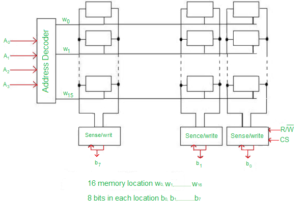
Internal Construction of Memory
Memory Decoding Process:
A memory decoding process is a multi-step process, where many addresses are used to identify the specific memory location. A memory decoding took place, where, there is a requirement to access the stored memory in digital electronics. In the following process.
Memory decoders are needed to select the memory-specified input addresses from the memory unit. Here the memory cell plays a vital role in the process.
The Memory cell: The cell is a kind of electric circuit, which contains four to six transistors. The selected input makes it easy for a cell to process read/write operations. In the process, by creating a line from the latch to the output terminal, A1 in the read/ write input performs the read operation. And on the other hand, by constructing the path from the input terminal to the latch, A0 in the read/write can perform the write operation.
As for the construction of the cell, usually, the memory cell is capable of storing binary signals in different units, which are known as bits. Initially, one bit equals 8 bits, and one word has a value of 2 bits. The data input and output lines communicate among the memory through the read/ write operations. Initially, it helps in determining the transfer of information. In memory, every word has a number, which is called address. These addresses range from 0 to 2k-1. Here, k refers to an address line number.
In general, a small RAM consists of four words of four bits each and a total of 16 binary cells. The binary cell, along with three inputs and one output, represents the small block cell (BC). Here, the user needs two address lines for the four memory words. To select one out of four words, the address inputs need to go through a 2:4 decoder, which can be enabled through the memory-enable input.
Going further in the process, in the condition of memory enabled value 0, all outputs in the decoder are turned 0 and none of them is selected. And if the memory selected value is 1, 1 out of the four words will be selected.
The Read/write operation: Here, after the selection of the word, the read/write input proceeds through the operation. In the process of reading operation, the four bits of the selected word pass through the OR gates to the output terminals.
On the other hand, in the write operation, the available data in the input lines are transferred into the four binary cells out of the selected word. During the process, the cells that are not selected turn dummy cells, and their values remain intact.
Memory Address Decoding:
In the random access memory, there is a free space, where thousands of word addresses are available. Each memory word has a value, which ranges from 1 up to 64 bits. Here, a memory within 2k words uses k memory address lines with n bits for each memory word. The decoder consists of 2k memory addresses, where each decoded address output identifies a single n-bit word for further reading or writing.
Here the address line represents the data input, which is known as code, the outputs represent a word signal, which can be either high or low. In PCs and microprocessors, there is a located memory chip, and every chip has a selected input. Now, to select, the memory chip needs to be specified.
When a single chip is selected and operated at the same time. It allows the user to select a correct memory address coded device for a certain memory address location.
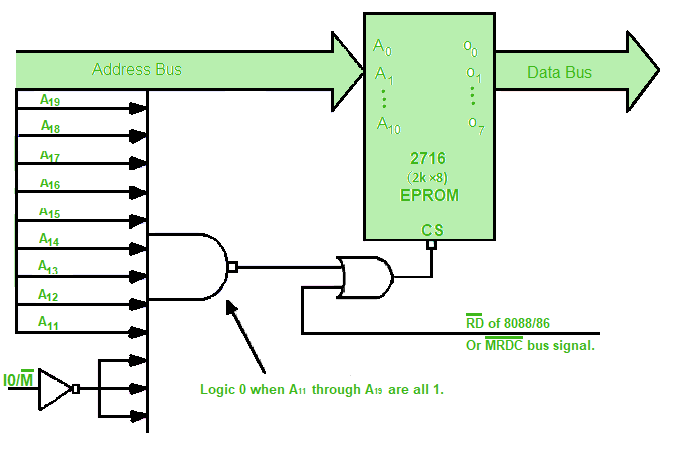
Example: Now as an example let’s take 8088, which creates 20-bit addresses for a 1MB memory address space as an output. On the other side, an EPROM BIOS 2716, has only 2KB memory along with 11 address pins. Now, here the EPROM can be placed in any 2KB section of the 1MB address space, as the decoder here can decode the extra 9 address pins.
This can be understood with the help of the following diagram:
Memory Decoding Circuit
Coincident Decoding:
In the coincident decoding, a decoder with k inputs creates the output with a 2k value. This type of decoder requires 2k AND gates, along with k inputs at each gate. Here, by combining two decoders into a two-dimensional scheme, the total number of gates and inputs per gate could be reduced.
Also, In the bi-dimensional matrix method, one of the decoders is used for row selection and the other for column selection. In this case, two 2k inputs are used instead of one k inputs.
This can be understood with the help of the following diagram:
Two-Dimensional Decoding Structure for a 1k-word memory
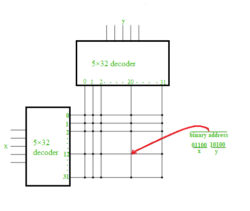
Example: Here, instead of using a 10 x 1,024 decoder in the selection method for 1K word of memory, two 5 x 32 decoders can be selected. We need 1,024 AND gates with ten inputs each in a single decoder.
In the case of two decoders, we would need 64 AND gates, each having five inputs. The first five most significant bits are assigned to the input X, and the last five least significant bits are assigned to the input Y. Every word in the memory array is chosen as the result of a coincidence of one X line and one Y input.
As a result, a single word in memory is chosen by the coincidence factor between 1 of 32 rows and 1 or 32 columns, for a total of nearly 1,024 words. The needed word is found at the intersection of a specific row and column. After then, all of the required word bits are read/written.
The Address Multiplexing:
Address multiplexing allows the user to use lesser pins and as a result, a few bus lines on the processor are used. Instead of having separate bus lines for the address and data, the address on the data line can be placed, where, the data is read and saved at the previously read address.
In detail, there are six transistors in SRAM or Static random-access memory. When the transistors are less in size, the high-density memory cells are created.
DRAM or Dynamic random-access memory, also includes a transistor, giving it a larger memory storage capacity than SRAM. SRAM data storage is more expensive than DRAM data storage. DRAM is more energy efficient.
Because the word bit size of DRAM is one, multiple chips are needed. Mainly because of the increased capacity; the decoding of all DRAM bits is performed in a two-dimensional array, and if there is more memory data in a cell, several arrays are needed. Address multiplexing is used by designers to reduce the number of pins in integrated circuits.
Here, the address is separated into two parts for separate groups of times in the two-dimensional array. The addresses for the rows are listed first, followed by the addresses for the columns. The total size is purposely decreased since the same pin set is used for both sides of the memory address.
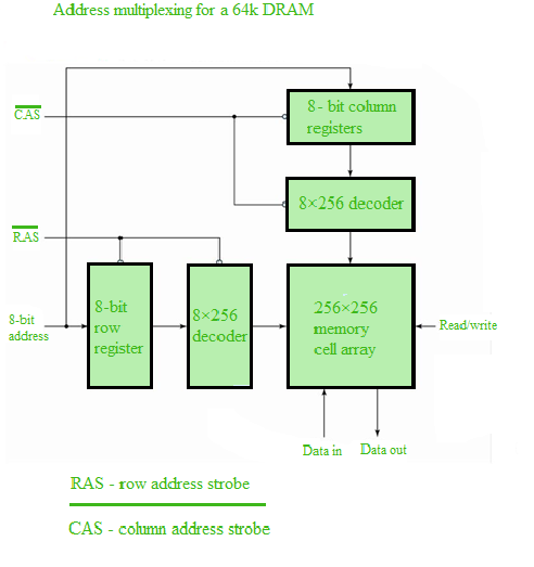
Example: In multiplexing, a 64K word memory is needed. The two-dimensional array of cells is organized into 256 rows and 256 columns, which then, makes the memory address. This gives a total of 64K words of memory There are two address strobes, a single data input line, a single data output line, a read/write control with an eight-bit address input, and a single data input line. The row addresses strobe abbreviated RAS, which activates the eight-bit memory row register. The column address strobe is truncated because CAS enables the 8-bit column register. The strobe symbol features a bar on top, indicating that the registers are either empty or at the signal’s zero level.
This can be understood with the following diagram:
The Diagram of Address multiplexing
So far, we’ve covered the internal construction and the memory decoding procedure, along with the different aspects of decoding in this article. Finally, we can say that memory decoding is an important yet fundamental aspect of accessing the memory of digital electronic circuitry.
«FlashROM» redirects here. For programming utility, see Flashrom (utility).
For the neuropsychological concept related to human memory, see Flashbulb memory.
Flash memory is an electronic non-volatile computer memory storage medium that can be electrically erased and reprogrammed. The two main types of flash memory, NOR flash and NAND flash, are named for the NOR and NAND logic gates. Both use the same cell design, consisting of floating gate MOSFETs. They differ at the circuit level depending on whether the state of the bit line or word lines is pulled high or low: in NAND flash, the relationship between the bit line and the word lines resembles a NAND gate; in NOR flash, it resembles a NOR gate.
Flash memory, a type of floating-gate memory, was invented at Toshiba in 1980 and is based on EEPROM technology. Toshiba began marketing flash memory in 1987.[1] had to be erased completely before they could be rewritten. NAND flash memory, however, may be erased, written, and read in blocks (or pages), which generally are much smaller than the entire device. NOR flash memory allows a single machine word to be written – to an erased location – or read independently. A flash memory device typically consists of one or more flash memory chips (each holding many flash memory cells), along with a separate flash memory controller chip.
The NAND type is found mainly in memory cards, USB flash drives, solid-state drives (those produced since 2009), feature phones, smartphones, and similar products, for general storage and transfer of data. NAND or NOR flash memory is also often used to store configuration data in digital products, a task previously made possible by EEPROM or battery-powered static RAM. A key disadvantage of flash memory is that it can endure only a relatively small number of write cycles in a specific block.[2]
Flash memory[3] is used in computers, PDAs, digital audio players, digital cameras, mobile phones, synthesizers, video games, scientific instrumentation, industrial robotics, and medical electronics. Flash memory has fast read access time, but it is not as fast as static RAM or ROM. In portable devices, it is preferred to use flash memory because of its mechanical shock resistance since mechanical drives are more prone to mechanical damage.[4]
Because erase cycles are slow, the large block sizes used in flash memory erasing give it a significant speed advantage over non-flash EEPROM when writing large amounts of data. As of 2019, flash memory costs much less[by how much?] than byte-programmable EEPROM and had become the dominant memory type wherever a system required a significant amount of non-volatile solid-state storage. EEPROMs, however, are still used in applications that require only small amounts of storage, as in serial presence detect.[5][6]
Flash memory packages can use die stacking with through-silicon vias and several dozen layers of 3D TLC NAND cells (per die) simultaneously to achieve capacities of up to 1 tebibyte per package using 16 stacked dies and an integrated flash controller as a separate die inside the package.[7][8][9][10]
HistoryEdit
BackgroundEdit
The origins of flash memory can be traced back to the development of the floating-gate MOSFET (FGMOS), also known as the floating-gate transistor.[11][12] The original MOSFET (metal–oxide–semiconductor field-effect transistor), also known as the MOS transistor, was invented by Egyptian engineer Mohamed M. Atalla and Korean engineer Dawon Kahng at Bell Labs in 1959.[13] Kahng went on to develop a variation, the floating-gate MOSFET, with Chinese engineer Simon Min Sze at Bell Labs in 1967.[14] They proposed that it could be used as floating-gate memory cells for storing a form of programmable read-only memory (PROM) that is both non-volatile and re-programmable.[14]
Early types of floating-gate memory included EPROM (erasable PROM) and EEPROM (electrically erasable PROM) in the 1970s.[14] However, early floating-gate memory required engineers to build a memory cell for each bit of data, which proved to be cumbersome,[15] slow,[16] and expensive, restricting floating-gate memory to niche applications in the 1970s, such as military equipment and the earliest experimental mobile phones.[11]
Invention and commercializationEdit
Fujio Masuoka, while working for Toshiba, proposed a new type of floating-gate memory that allowed entire sections of memory to be erased quickly and easily, by applying a voltage to a single wire connected to a group of cells.[11] This led to Masuoka’s invention of flash memory at Toshiba in 1980.[15][17][18] According to Toshiba, the name «flash» was suggested by Masuoka’s colleague, Shōji Ariizumi, because the erasure process of the memory contents reminded him of the flash of a camera.[19] Masuoka and colleagues presented the invention of NOR flash in 1984,[20][21] and then NAND flash at the IEEE 1987 International Electron Devices Meeting (IEDM) held in San Francisco.[22]
Toshiba commercially launched NAND flash memory in 1987.[1][14] Intel Corporation introduced the first commercial NOR type flash chip in 1988.[23] NOR-based flash has long erase and write times, but provides full address and data buses, allowing random access to any memory location. This makes it a suitable replacement for older read-only memory (ROM) chips, which are used to store program code that rarely needs to be updated, such as a computer’s BIOS or the firmware of set-top boxes. Its endurance may be from as little as 100 erase cycles for an on-chip flash memory,[24] to a more typical 10,000 or 100,000 erase cycles, up to 1,000,000 erase cycles.[25] NOR-based flash was the basis of early flash-based removable media; CompactFlash was originally based on it, though later cards moved to less expensive NAND flash.
NAND flash has reduced erase and write times, and requires less chip area per cell, thus allowing greater storage density and lower cost per bit than NOR flash. However, the I/O interface of NAND flash does not provide a random-access external address bus. Rather, data must be read on a block-wise basis, with typical block sizes of hundreds to thousands of bits. This makes NAND flash unsuitable as a drop-in replacement for program ROM, since most microprocessors and microcontrollers require byte-level random access. In this regard, NAND flash is similar to other secondary data storage devices, such as hard disks and optical media, and is thus highly suitable for use in mass-storage devices, such as memory cards and solid-state drives (SSD). Flash memory cards and SSDs store data using multiple NAND flash memory chips.
The first NAND-based removable memory card format was SmartMedia, released in 1995. Many others followed, including MultiMediaCard, Secure Digital, Memory Stick, and xD-Picture Card.
Later developmentsEdit
A new generation of memory card formats, including RS-MMC, miniSD and microSD, feature extremely small form factors. For example, the microSD card has an area of just over 1.5 cm2, with a thickness of less than 1 mm.
NAND flash has achieved significant levels of memory density as a result of several major technologies that were commercialized during the late 2000s to early 2010s.[26]
Multi-level cell (MLC) technology stores more than one bit in each memory cell. NEC demonstrated multi-level cell (MLC) technology in 1998, with an 80 Mb flash memory chip storing 2 bits per cell.[27] STMicroelectronics also demonstrated MLC in 2000, with a 64 MB NOR flash memory chip.[28] In 2009, Toshiba and SanDisk introduced NAND flash chips with QLC technology storing 4 bits per cell and holding a capacity of 64 Gbit.[29][30] Samsung Electronics introduced triple-level cell (TLC) technology storing 3-bits per cell, and began mass-producing NAND chips with TLC technology in 2010.[31]
Charge trap flashEdit
Charge trap flash (CTF) technology replaces the polysilicon floating gate, which is sandwiched between a blocking gate oxide above and a tunneling oxide below it, with an electrically insulating silicon nitride layer; the silicon nitride layer traps electrons. In theory, CTF is less prone to electron leakage, providing improved data retention.[32][33][34][35][36][37]
Because CTF replaces the polysilicon with an electrically insulating nitride, it allows for smaller cells and higher endurance (lower degradation or wear). However, electrons can become trapped and accumulate in the nitride, leading to degradation. Leakage is exacerbated at high temperatures since electrons become more excitated with increasing temperatures. CTF technology however still uses a tunneling oxide and blocking layer which are the weak points of the technology, since they can still be damaged in the usual ways (the tunnel oxide can be degraded due to extremely high electric fields and the blocking layer due to Anode Hot Hole Injection (AHHI).[38][39]
Degradation or wear of the oxides is the reason why flash memory has limited endurance, and data retention goes down (the potential for data loss increases) with increasing degradation, since the oxides lose their electrically insulating characteristics as they degrade. The oxides must insulate against electrons to prevent them from leaking which would cause data loss.
In 1991, NEC researchers including N. Kodama, K. Oyama and Hiroki Shirai described a type of flash memory with a charge trap method.[40] In 1998, Boaz Eitan of Saifun Semiconductors (later acquired by Spansion) patented a flash memory technology named NROM that took advantage of a charge trapping layer to replace the conventional floating gate used in conventional flash memory designs.[41] In 2000, an Advanced Micro Devices (AMD) research team led by Richard M. Fastow, Egyptian engineer Khaled Z. Ahmed and Jordanian engineer Sameer Haddad (who later joined Spansion) demonstrated a charge-trapping mechanism for NOR flash memory cells.[42] CTF was later commercialized by AMD and Fujitsu in 2002.[43] 3D V-NAND (vertical NAND) technology stacks NAND flash memory cells vertically within a chip using 3D charge trap flash (CTP) technology. 3D V-NAND technology was first announced by Toshiba in 2007,[44] and the first device, with 24 layers, was first commercialized by Samsung Electronics in 2013.[45][46]
3D integrated circuit technologyEdit
3D integrated circuit (3D IC) technology stacks integrated circuit (IC) chips vertically into a single 3D IC chip package.[26] Toshiba introduced 3D IC technology to NAND flash memory in April 2007, when they debuted a 16 GB eMMC compliant (product number THGAM0G7D8DBAI6, often abbreviated THGAM on consumer websites) embedded NAND flash memory chip, which was manufactured with eight stacked 2 GB NAND flash chips.[47] In September 2007, Hynix Semiconductor (now SK Hynix) introduced 24-layer 3D IC technology, with a 16 GB flash memory chip that was manufactured with 24 stacked NAND flash chips using a wafer bonding process.[48] Toshiba also used an eight-layer 3D IC for their 32 GB THGBM flash chip in 2008.[49] In 2010, Toshiba used a 16-layer 3D IC for their 128 GB THGBM2 flash chip, which was manufactured with 16 stacked 8 GB chips.[50] In the 2010s, 3D ICs came into widespread commercial use for NAND flash memory in mobile devices.[26]
As of August 2017, microSD cards with a capacity up to 400 GB (400 billion bytes) are available.[51][52] The same year, Samsung combined 3D IC chip stacking with its 3D V-NAND and TLC technologies to manufacture its 512 GB KLUFG8R1EM flash memory chip with eight stacked 64-layer V-NAND chips.[53] In 2019, Samsung produced a 1024 GB flash chip, with eight stacked 96-layer V-NAND chips and with QLC technology.[54][55]
Principles of operationEdit
Flash memory stores information in an array of memory cells made from floating-gate transistors. In single-level cell (SLC) devices, each cell stores only one bit of information. Multi-level cell (MLC) devices, including triple-level cell (TLC) devices, can store more than one bit per cell.
The floating gate may be conductive (typically polysilicon in most kinds of flash memory) or non-conductive (as in SONOS flash memory).[56]
Floating-gate MOSFETEdit
In flash memory, each memory cell resembles a standard metal–oxide–semiconductor field-effect transistor (MOSFET) except that the transistor has two gates instead of one. The cells can be seen as an electrical switch in which current flows between two terminals (source and drain) and is controlled by a floating gate (FG) and a control gate (CG). The CG is similar to the gate in other MOS transistors, but below this, there is the FG insulated all around by an oxide layer. The FG is interposed between the CG and the MOSFET channel. Because the FG is electrically isolated by its insulating layer, electrons placed on it are trapped. When the FG is charged with electrons, this charge screens the electric field from the CG, thus, increasing the threshold voltage (VT) of the cell. This means that the VT of the cell can be changed between the uncharged FG threshold voltage (VT1) and the higher charged FG threshold voltage (VT2) by changing the FG charge. In order to read a value from the cell, an intermediate voltage (VI) between VT1 and VT2 is applied to the CG. If the channel conducts at VI, the FG must be uncharged (if it were charged, there would not be conduction because VI is less than VT2). If the channel does not conduct at the VI, it indicates that the FG is charged. The binary value of the cell is sensed by determining whether there is current flowing through the transistor when VI is asserted on the CG. In a multi-level cell device, which stores more than one bit per cell, the amount of current flow is sensed (rather than simply its presence or absence), in order to determine more precisely the level of charge on the FG.
Floating gate MOSFETs are so named because there is an electrically insulating tunnel oxide layer between the floating gate and the silicon, so the gate «floats» above the silicon. The oxide keeps the electrons confined to the floating gate. Degradation or wear (and the limited endurance of floating gate Flash memory) occurs due to the extremely high electric field (10 million volts per centimeter) experienced by the oxide. Such high voltage densities can break atomic bonds over time in the relatively thin oxide, gradually degrading its electrically insulating properties and allowing electrons to be trapped in and pass through freely (leak) from the floating gate into the oxide, increasing the likelihood of data loss since the electrons (the quantity of which is used to represent different charge levels, each assigned to a different combination of bits in MLC Flash) are normally in the floating gate. This is why data retention goes down and the risk of data loss increases with increasing degradation.[57][58][36][59][60]The silicon oxide in a cell degrades with every erase operation. The degradation increases the amount of negative charge in the cell over time due to trapped electrons in the oxide and negates some of the control gate voltage, this over time also makes erasing the cell slower, so to maintain the performance and reliability of the NAND chip, the cell must be retired from use. Endurance also decreases with the number of bits in a cell. With more bits in a cell, the number of possible states (each represented by a different voltage level) in a cell increases and is more sensitive to the voltages used for programming. Voltages may be adjusted to compensate for degradation of the silicon oxide, and as the number of bits increases, the number of possible states also increases and thus the cell is less tolerant of adjustments to programming voltages, because there is less space between the voltage levels that define each state in a cell.[61]
Fowler–Nordheim tunnelingEdit
The process of moving electrons from the control gate and into the floating gate is called Fowler–Nordheim tunneling, and it fundamentally changes the characteristics of the cell by increasing the MOSFET’s threshold voltage. This, in turn, changes the drain-source current that flows through the transistor for a given gate voltage, which is ultimately used to encode a binary value. The Fowler-Nordheim tunneling effect is reversible, so electrons can be added to or removed from the floating gate, processes traditionally known as writing and erasing.[62]
Internal charge pumpsEdit
Despite the need for relatively high programming and erasing voltages, virtually all flash chips today require only a single supply voltage and produce the high voltages that are required using on-chip charge pumps.
Over half the energy used by a 1.8 V NAND flash chip is lost in the charge pump itself. Since boost converters are inherently more efficient than charge pumps, researchers developing low-power SSDs have proposed returning to the dual Vcc/Vpp supply voltages used on all early flash chips, driving the high Vpp voltage for all flash chips in an SSD with a single shared external boost converter.[63][64][65][66][67][68][69][70]
In spacecraft and other high-radiation environments, the on-chip charge pump is the first part of the flash chip to fail, although flash memories will continue to work – in read-only mode – at much higher radiation levels.[71]
NOR flashEdit
NOR flash memory wiring and structure on silicon
In NOR flash, each cell has one end connected directly to ground, and the other end connected directly to a bit line. This arrangement is called «NOR flash» because it acts like a NOR gate: when one of the word lines (connected to the cell’s CG) is brought high, the corresponding storage transistor acts to pull the output bit line low. NOR flash continues to be the technology of choice for embedded applications requiring a discrete non-volatile memory device.[citation needed] The low read latencies characteristic of NOR devices allow for both direct code execution and data storage in a single memory product.[72]
ProgrammingEdit
Programming a NOR memory cell (setting it to logical 0), via hot-electron injection
Erasing a NOR memory cell (setting it to logical 1), via quantum tunneling
A single-level NOR flash cell in its default state is logically equivalent to a binary «1» value, because current will flow through the channel under application of an appropriate voltage to the control gate, so that the bitline voltage is pulled down. A NOR flash cell can be programmed, or set to a binary «0» value, by the following procedure:
- an elevated on-voltage (typically >5 V) is applied to the CG
- the channel is now turned on, so electrons can flow from the source to the drain (assuming an NMOS transistor)
- the source-drain current is sufficiently high to cause some high energy electrons to jump through the insulating layer onto the FG, via a process called hot-electron injection.
ErasingEdit
To erase a NOR flash cell (resetting it to the «1» state), a large voltage of the opposite polarity is applied between the CG and source terminal, pulling the electrons off the FG through quantum tunneling. Modern NOR flash memory chips are divided into erase segments (often called blocks or sectors). The erase operation can be performed only on a block-wise basis; all the cells in an erase segment must be erased together. Programming of NOR cells, however, generally can be performed one byte or word at a time.
NAND flash memory wiring and structure on silicon
NAND flashEdit
NAND flash also uses floating-gate transistors, but they are connected in a way that resembles a NAND gate: several transistors are connected in series, and the bit line is pulled low only if all the word lines are pulled high (above the transistors’ VT). These groups are then connected via some additional transistors to a NOR-style bit line array in the same way that single transistors are linked in NOR flash.
Compared to NOR flash, replacing single transistors with serial-linked groups adds an extra level of addressing. Whereas NOR flash might address memory by page then word, NAND flash might address it by page, word and bit. Bit-level addressing suits bit-serial applications (such as hard disk emulation), which access only one bit at a time. Execute-in-place applications, on the other hand, require every bit in a word to be accessed simultaneously. This requires word-level addressing. In any case, both bit and word addressing modes are possible with either NOR or NAND flash.
To read data, first the desired group is selected (in the same way that a single transistor is selected from a NOR array). Next, most of the word lines are pulled up above VT2, while one of them is pulled up to VI. The series group will conduct (and pull the bit line low) if the selected bit has not been programmed.
Despite the additional transistors, the reduction in ground wires and bit lines allows a denser layout and greater storage capacity per chip. (The ground wires and bit lines are actually much wider than the lines in the diagrams.) In addition, NAND flash is typically permitted to contain a certain number of faults (NOR flash, as is used for a BIOS ROM, is expected to be fault-free). Manufacturers try to maximize the amount of usable storage by shrinking the size of the transistors.
NAND Flash cells are read by analysing their response to various voltages.[59]
Writing and erasingEdit
NAND flash uses tunnel injection for writing and tunnel release for erasing. NAND flash memory forms the core of the removable USB storage devices known as USB flash drives, as well as most memory card formats and solid-state drives available today.
The hierarchical structure of NAND flash starts at a cell level which establishes strings, then pages, blocks, planes and ultimately a die. A string is a series of connected NAND cells in which the source of one cell is connected to the drain of the next one. Depending on the NAND technology, a string typically consists of 32 to 128 NAND cells. Strings are organised into pages which are then organised into blocks in which each string is connected to a separate line called a bitline. All cells with the same position in the string are connected through the control gates by a wordline. A plane contains a certain number of blocks that are connected through the same bitline. A flash die consists of one or more planes, and the peripheral circuitry that is needed to perform all the read, write, and erase operations.
The architecture of NAND flash means that data can be read and programmed (written) in pages, typically between 4 KiB and 16 KiB in size, but can only be erased at the level of entire blocks consisting of multiple pages. When a block is erased, all the cells are logically set to 1. Data can only be programmed in one pass to a page in a block that was erased. Any cells that have been set to 0 by programming can only be reset to 1 by erasing the entire block. This means that before new data can be programmed into a page that already contains data, the current contents of the page plus the new data must be copied to a new, erased page. If a suitable erased page is available, the data can be written to it immediately. If no erased page is available, a block must be erased before copying the data to a page in that block. The old page is then marked as invalid and is available for erasing and reuse.[73]
Vertical NANDEdit
3D NAND continues scaling beyond 2D.
Vertical NAND (V-NAND) or 3D NAND memory stacks memory cells vertically and uses a charge trap flash architecture. The vertical layers allow larger areal bit densities without requiring smaller individual cells.[74] It is also sold under the trademark BiCS Flash, which is a trademark of Kioxia Corporation (former Toshiba Memory Corporation). 3D NAND was first announced by Toshiba in 2007.[44] V-NAND was first commercially manufactured by Samsung Electronics in 2013.[45][46][75][76]
StructureEdit
V-NAND uses a charge trap flash geometry (which was commercially introduced in 2002 by AMD and Fujitsu)[43] that stores charge on an embedded silicon nitride film. Such a film is more robust against point defects and can be made thicker to hold larger numbers of electrons. V-NAND wraps a planar charge trap cell into a cylindrical form.[74] As of 2020, 3D NAND Flash memories by Micron and Intel instead use floating gates, however, Micron 128 layer and above 3D NAND memories use a conventional charge trap structure, due to the dissolution of the partnership between Micron and Intel. Charge trap 3D NAND Flash is thinner than floating gate 3D NAND. In floating gate 3D NAND, the memory cells are completely separated from one another, whereas in charge trap 3D NAND, vertical groups of memory cells share the same silicon nitride material.[77]
An individual memory cell is made up of one planar polysilicon layer containing a hole filled by multiple concentric vertical cylinders. The hole’s polysilicon surface acts as the gate electrode. The outermost silicon dioxide cylinder acts as the gate dielectric, enclosing a silicon nitride cylinder that stores charge, in turn enclosing a silicon dioxide cylinder as the tunnel dielectric that surrounds a central rod of conducting polysilicon which acts as the conducting channel.[74]
Memory cells in different vertical layers do not interfere with each other, as the charges cannot move vertically through the silicon nitride storage medium, and the electric fields associated with the gates are closely confined within each layer. The vertical collection is electrically identical to the serial-linked groups in which conventional NAND flash memory is configured.[74]
ConstructionEdit
Growth of a group of V-NAND cells begins with an alternating stack of conducting (doped) polysilicon layers and insulating silicon dioxide layers.[74]
The next step is to form a cylindrical hole through these layers. In practice, a 128 Gibit V-NAND chip with 24 layers of memory cells requires about 2.9 billion such holes. Next, the hole’s inner surface receives multiple coatings, first silicon dioxide, then silicon nitride, then a second layer of silicon dioxide. Finally, the hole is filled with conducting (doped) polysilicon.[74]
PerformanceEdit
As of 2013, V-NAND flash architecture allows read and write operations twice as fast as conventional NAND and can last up to 10 times as long, while consuming 50 percent less power. They offer comparable physical bit density using 10-nm lithography but may be able to increase bit density by up to two orders of magnitude, given V-NAND’s use of up to several hundred layers.[74] As of 2020, V-NAND chips with 160 layers are under development by Samsung.[78]
CostEdit
Minimum bit cost of 3D NAND from non-vertical sidewall. The top opening widens with more layers, counteracting the increase in bit density.
The wafer cost of a 3D NAND is comparable with scaled down (32 nm or less) planar NAND Flash.[79] However, with planar NAND scaling stopping at 16 nm, the cost per bit reduction can continue by 3D NAND starting with 16 layers. However, due to the non-vertical sidewall of the hole etched through the layers; even a slight deviation leads to a minimum bit cost, i.e., minimum equivalent design rule (or maximum density), for a given number of layers; this minimum bit cost layer number decreases for smaller hole diameter.[80]
LimitationsEdit
Block erasureEdit
One limitation of flash memory is that it can be erased only a block at a time. This generally sets all bits in the block to 1. Starting with a freshly erased block, any location within that block can be programmed. However, once a bit has been set to 0, only by erasing the entire block can it be changed back to 1. In other words, flash memory (specifically NOR flash) offers random-access read and programming operations but does not offer arbitrary random-access rewrite or erase operations. A location can, however, be rewritten as long as the new value’s 0 bits are a superset of the over-written values. For example, a nibble value may be erased to 1111, then written as 1110. Successive writes to that nibble can change it to 1010, then 0010, and finally 0000. Essentially, erasure sets all bits to 1, and programming can only clear bits to 0.[81]
Some file systems designed for flash devices make use of this rewrite capability, for example Yaffs1, to represent sector metadata.
Other flash file systems, such as YAFFS2, never make use of this «rewrite» capability—they do a lot of extra work to meet a «write once rule».
Although data structures in flash memory cannot be updated in completely general ways, this allows members to be «removed» by marking them as invalid. This technique may need to be modified for multi-level cell devices, where one memory cell holds more than one bit.
Common flash devices such as USB flash drives and memory cards provide only a block-level interface, or flash translation layer (FTL), which writes to a different cell each time to wear-level the device. This prevents incremental writing within a block; however, it does help the device from being prematurely worn out by intensive write patterns.
Data RetentionEdit
45nm NOR flash memory example of data retention varying with temperatures
Data stored on flash cells is steadily lost due to electron detrapping[definition needed]. The rate of loss increases exponentially as the absolute temperature increases. For example: For a 45 nm NOR Flash, at 1000 hours, the threshold voltage (Vt) loss at 25 deg Celsius is about half that at 90 deg Celsius.[82]
Memory wearEdit
Another limitation is that flash memory has a finite number of program – erase cycles (typically written as P/E cycles). [83][84] Micron Technology and Sun Microsystems announced an SLC NAND flash memory chip rated for 1,000,000 P/E cycles on 17 December 2008.[85] Longer P/E cycles of Industrial SSDs speak for their endurance level and make them more reliable for Industrial usage.
The guaranteed cycle count may apply only to block zero (as is the case with TSOP NAND devices), or to all blocks (as in NOR). This effect is mitigated in some chip firmware or file system drivers by counting the writes and dynamically remapping blocks in order to spread write operations between sectors; this technique is called wear leveling. Another approach is to perform write verification and remapping to spare sectors in case of write failure, a technique called bad block management (BBM). For portable consumer devices, these wear out management techniques typically extend the life of the flash memory beyond the life of the device itself, and some data loss may be acceptable in these applications. For high-reliability data storage, however, it is not advisable to use flash memory that would have to go through a large number of programming cycles. This limitation is meaningless for ‘read-only’ applications such as thin clients and routers, which are programmed only once or at most a few times during their lifetimes.
In December 2012, Taiwanese engineers from Macronix revealed their intention to announce at the 2012 IEEE International Electron Devices Meeting that they had figured out how to improve NAND flash storage read/write cycles from 10,000 to 100 million cycles using a «self-healing» process that used a flash chip with «onboard heaters that could anneal small groups of memory cells.»[86] The built-in thermal annealing was to replace the usual erase cycle with a local high temperature process that not only erased the stored charge, but also repaired the electron-induced stress in the chip, giving write cycles of at least 100 million.[87] The result was to be a chip that could be erased and rewritten over and over, even when it should theoretically break down. As promising as Macronix’s breakthrough might have been for the mobile industry, however, there were no plans for a commercial product featuring this capability to be released any time in the near future.[88]
Read disturbEdit
The method used to read NAND flash memory can cause nearby cells in the same memory block to change over time (become programmed). This is known as read disturb. The threshold number of reads is generally in the hundreds of thousands of reads between intervening erase operations. If reading continually from one cell, that cell will not fail but rather one of the surrounding cells on a subsequent read. To avoid the read disturb problem the flash controller will typically count the total number of reads to a block since the last erase. When the count exceeds a target limit, the affected block is copied over to a new block, erased, then released to the block pool. The original block is as good as new after the erase. If the flash controller does not intervene in time, however, a read disturb error will occur with possible data loss if the errors are too numerous to correct with an error-correcting code.[89][90][91]
X-ray effectsEdit
Most flash ICs come in ball grid array (BGA) packages, and even the ones that do not are often mounted on a PCB next to other BGA packages. After PCB Assembly, boards with BGA packages are often X-rayed to see if the balls are making proper connections to the proper pad, or if the BGA needs rework. These X-rays can erase programmed bits in a flash chip (convert programmed «0» bits into erased «1» bits). Erased bits («1» bits) are not affected by X-rays.[92][93]
Some manufacturers are now making X-ray proof SD[94] and USB[95] memory devices.
Low-level accessEdit
The low-level interface to flash memory chips differs from those of other memory types such as DRAM, ROM, and EEPROM, which support bit-alterability (both zero to one and one to zero) and random access via externally accessible address buses.
NOR memory has an external address bus for reading and programming. For NOR memory, reading and programming are random-access, and unlocking and erasing are block-wise. For NAND memory, reading and programming are page-wise, and unlocking and erasing are block-wise.
NOR memoriesEdit
Reading from NOR flash is similar to reading from random-access memory, provided the address and data bus are mapped correctly. Because of this, most microprocessors can use NOR flash memory as execute in place (XIP) memory, meaning that programs stored in NOR flash can be executed directly from the NOR flash without needing to be copied into RAM first. NOR flash may be programmed in a random-access manner similar to reading. Programming changes bits from a logical one to a zero. Bits that are already zero are left unchanged. Erasure must happen a block at a time, and resets all the bits in the erased block back to one. Typical block sizes are 64, 128, or 256 KiB.
Bad block management is a relatively new feature in NOR chips. In older NOR devices not supporting bad block management, the software or device driver controlling the memory chip must correct for blocks that wear out, or the device will cease to work reliably.
The specific commands used to lock, unlock, program, or erase NOR memories differ for each manufacturer. To avoid needing unique driver software for every device made, special Common Flash Memory Interface (CFI) commands allow the device to identify itself and its critical operating parameters.
Besides its use as random-access ROM, NOR flash can also be used as a storage device, by taking advantage of random-access programming. Some devices offer read-while-write functionality so that code continues to execute even while a program or erase operation is occurring in the background. For sequential data writes, NOR flash chips typically have slow write speeds, compared with NAND flash.
Typical NOR flash does not need an error correcting code.[96]
NAND memoriesEdit
NAND flash architecture was introduced by Toshiba in 1989.[97] These memories are accessed much like block devices, such as hard disks. Each block consists of a number of pages. The pages are typically 512,[98] 2,048 or 4,096 bytes in size. Associated with each page are a few bytes (typically 1/32 of the data size) that can be used for storage of an error correcting code (ECC) checksum.
Typical block sizes include:
- 32 pages of 512+16 bytes each for a block size (effective) of 16 KiB
- 64 pages of 2,048+64 bytes each for a block size of 128 KiB[99]
- 64 pages of 4,096+128 bytes each for a block size of 256 KiB[100]
- 128 pages of 4,096+128 bytes each for a block size of 512 KiB.
While reading and programming is performed on a page basis, erasure can only be performed on a block basis.[101]
NAND devices also require bad block management by the device driver software or by a separate controller chip. Some SD cards, for example, include controller circuitry to perform bad block management and wear leveling. When a logical block is accessed by high-level software, it is mapped to a physical block by the device driver or controller. A number of blocks on the flash chip may be set aside for storing mapping tables to deal with bad blocks, or the system may simply check each block at power-up to create a bad block map in RAM. The overall memory capacity gradually shrinks as more blocks are marked as bad.
NAND relies on ECC to compensate for bits that may spontaneously fail during normal device operation. A typical ECC will correct a one-bit error in each 2048 bits (256 bytes) using 22 bits of ECC, or a one-bit error in each 4096 bits (512 bytes) using 24 bits of ECC.[102] If the ECC cannot correct the error during read, it may still detect the error. When doing erase or program operations, the device can detect blocks that fail to program or erase and mark them bad. The data is then written to a different, good block, and the bad block map is updated.
Hamming codes are the most commonly used ECC for SLC NAND flash. Reed-Solomon codes and BCH codes (Bose-Chaudhuri-Hocquenghem codes) are commonly used ECC for MLC NAND flash. Some MLC NAND flash chips internally generate the appropriate BCH error correction codes.[96]
Most NAND devices are shipped from the factory with some bad blocks. These are typically marked according to a specified bad block marking strategy. By allowing some bad blocks, manufacturers achieve far higher yields than would be possible if all blocks had to be verified to be good. This significantly reduces NAND flash costs and only slightly decreases the storage capacity of the parts.
When executing software from NAND memories, virtual memory strategies are often used: memory contents must first be paged or copied into memory-mapped RAM and executed there (leading to the common combination of NAND + RAM). A memory management unit (MMU) in the system is helpful, but this can also be accomplished with overlays. For this reason, some systems will use a combination of NOR and NAND memories, where a smaller NOR memory is used as software ROM and a larger NAND memory is partitioned with a file system for use as a non-volatile data storage area.
NAND sacrifices the random-access and execute-in-place advantages of NOR. NAND is best suited to systems requiring high capacity data storage. It offers higher densities, larger capacities, and lower cost. It has faster erases, sequential writes, and sequential reads.
StandardizationEdit
A group called the Open NAND Flash Interface Working Group (ONFI) has developed a standardized low-level interface for NAND flash chips. This allows interoperability between conforming NAND devices from different vendors. The ONFI specification version 1.0[103] was released on 28 December 2006. It specifies:
- A standard physical interface (pinout) for NAND flash in TSOP-48, WSOP-48, LGA-52, and BGA-63 packages
- A standard command set for reading, writing, and erasing NAND flash chips
- A mechanism for self-identification (comparable to the serial presence detection feature of SDRAM memory modules)
The ONFI group is supported by major NAND flash manufacturers, including Hynix, Intel, Micron Technology, and Numonyx, as well as by major manufacturers of devices incorporating NAND flash chips.[104]
Two major flash device manufacturers, Toshiba and Samsung, have chosen to use an interface of their own design known as Toggle Mode (and now Toggle). This interface isn’t pin-to-pin compatible with the ONFI specification. The result is that a product designed for one vendor’s devices may not be able to use another vendor’s devices.[105]
A group of vendors, including Intel, Dell, and Microsoft, formed a Non-Volatile Memory Host Controller Interface (NVMHCI) Working Group.[106] The goal of the group is to provide standard software and hardware programming interfaces for nonvolatile memory subsystems, including the «flash cache» device connected to the PCI Express bus.
Distinction between NOR and NAND flashEdit
NOR and NAND flash differ in two important ways:
- The connections of the individual memory cells are different.[citation needed]
- The interface provided for reading and writing the memory is different; NOR allows random access, while NAND allows only page access.[107]
NOR and NAND flash get their names from the structure of the interconnections between memory cells.[citation needed] In NOR flash, cells are connected in parallel to the bit lines, allowing cells to be read and programmed individually. The parallel connection of cells resembles the parallel connection of transistors in a CMOS NOR gate. In NAND flash, cells are connected in series, resembling a CMOS NAND gate. The series connections consume less space than parallel ones, reducing the cost of NAND flash. It does not, by itself, prevent NAND cells from being read and programmed individually.[citation needed]
Each NOR flash cell is larger than a NAND flash cell – 10 F2 vs 4 F2 – even when using exactly the same semiconductor device fabrication and so each transistor, contact, etc. is exactly the same size – because NOR flash cells require a separate metal contact for each cell.[108]
Because of the series connection and removal of wordline contacts, a large grid of NAND flash memory cells will occupy perhaps only 60% of the area of equivalent NOR cells[109] (assuming the same CMOS process resolution, for example, 130 nm, 90 nm, or 65 nm). NAND flash’s designers realized that the area of a NAND chip, and thus the cost, could be further reduced by removing the external address and data bus circuitry. Instead, external devices could communicate with NAND flash via sequential-accessed command and data registers, which would internally retrieve and output the necessary data. This design choice made random-access of NAND flash memory impossible, but the goal of NAND flash was to replace mechanical hard disks, not to replace ROMs.
| Attribute | NAND | NOR |
|---|---|---|
| Main application | File storage | Code execution |
| Storage capacity | High | Low |
| Cost per bit | Low | |
| Active power | Low | |
| Standby power | Low | |
| Write speed | Fast | |
| Read speed | Fast | |
| Execute in place (XIP) | No | Yes |
| Reliability | High |
Write enduranceEdit
The write endurance of SLC floating-gate NOR flash is typically equal to or greater than that of NAND flash, while MLC NOR and NAND flash have similar endurance capabilities. Examples of endurance cycle ratings listed in datasheets for NAND and NOR flash, as well as in storage devices using flash memory, are provided.[110]
| Type of flash memory |
Endurance rating (erases per block) |
Example(s) of flash memory or storage device |
|---|---|---|
| SLC NAND | 100,000 | Samsung OneNAND KFW4G16Q2M, Toshiba SLC NAND Flash chips,[111][112][113][114][115] Transcend SD500, Fujitsu S26361-F3298 |
| MLC NAND | 5,000–10,000 for medium-capacity; 1,000 to 3,000 for high-capacity[116] |
Samsung K9G8G08U0M (Example for medium-capacity applications), Memblaze PBlaze4,[117] ADATA SU900, Mushkin Reactor |
| TLC NAND | 1,000 | Samsung SSD 840 |
| QLC NAND | unknown | SanDisk X4 NAND flash SD cards[118][119][120][121] |
| 3D SLC NAND | 100,000 | Samsung Z-NAND[122] |
| 3D MLC NAND | 6,000–40,000 | Samsung SSD 850 PRO, Samsung SSD 845DC PRO,[123][124] Samsung 860 PRO |
| 3D TLC NAND | 1,000–3,000 | Samsung SSD 850 EVO, Samsung SSD 845DC EVO, Crucial MX300[125][126][127],Memblaze PBlaze5 900, Memblaze PBlaze5 700, Memblaze PBlaze5 910/916,Memblaze PBlaze5 510/516,[128][129][130][131] ADATA SX 8200 PRO (also being sold under «XPG Gammix» branding, model S11 PRO) |
| 3D QLC NAND | 100–1,000 | Samsung SSD 860 QVO SATA, Intel SSD 660p, Samsung SSD 980 QVO NVMe, Micron 5210 ION, Samsung SSD BM991 NVMe[132][133][134][135][136][137][138][139] |
| 3D PLC NAND | unknown | In development by SK Hynix (formerly Intel)[140] and Kioxia (formerly Toshiba Memory).[116] |
| SLC (floating- gate) NOR |
100,000–1,000,000 | Numonyx M58BW (Endurance rating of 100,000 erases per block); Spansion S29CD016J (Endurance rating of 1,000,000 erases per block) |
| MLC (floating- gate) NOR |
100,000 | Numonyx J3 flash |
However, by applying certain algorithms and design paradigms such as wear leveling and memory over-provisioning, the endurance of a storage system can be tuned to serve specific requirements.[141]
In order to compute the longevity of the NAND flash, one must account for the size of the memory chip, the type of memory (e.g. SLC/MLC/TLC), and use pattern. Industrial NAND are in demand due to their capacity, longer endurance and reliability in sensitive environments.
3D NAND performance may degrade as layers are added.[122]
As the number of bits per cell increases, the performance of NAND flash may degrade, increasing random read times to 100μs for TLC NAND which is 4 times the time required in SLC NAND, and twice the time required in MLC NAND, for random reads.[61]
Flash file systemsEdit
Because of the particular characteristics of flash memory, it is best used with either a controller to perform wear leveling and error correction or specifically designed flash file systems, which spread writes over the media and deal with the long erase times of NOR flash blocks. The basic concept behind flash file systems is the following: when the flash store is to be updated, the file system will write a new copy of the changed data to a fresh block, remap the file pointers, then erase the old block later when it has time.
In practice, flash file systems are used only for memory technology devices (MTDs), which are embedded flash memories that do not have a controller. Removable flash memory cards, SSDs, eMMC/eUFS chips and USB flash drives have built-in controllers to perform wear leveling and error correction so use of a specific flash file system may not add benefit.
CapacityEdit
Multiple chips are often arrayed or die stacked to achieve higher capacities[142] for use in consumer electronic devices such as multimedia players or GPSs. The capacity scaling (increase) of flash chips used to follow Moore’s law because they are manufactured with many of the same integrated circuits techniques and equipment. Since the introduction of 3D NAND, scaling is no longer necessarily associated with Moore’s law since ever smaller transistors (cells) are no longer used.
Consumer flash storage devices typically are advertised with usable sizes expressed as a small integer power of two (2, 4, 8, etc.) and a conventional designation of megabytes (MB) or gigabytes (GB); e.g., 512 MB, 8 GB. This includes SSDs marketed as hard drive replacements, in accordance with traditional hard drives, which use decimal prefixes.[143] Thus, an SSD marked as «64 GB» is at least 64 × 10003 bytes (64 GB). Most users will have slightly less capacity than this available for their files, due to the space taken by file system metadata and because some operating systems report SSD capacity using binary prefixes which are somewhat larger than conventional prefixes .
The flash memory chips inside them are sized in strict binary multiples, but the actual total capacity of the chips is not usable at the drive interface.
It is considerably larger than the advertised capacity in order to allow for distribution of writes (wear leveling), for sparing, for error correction codes, and for other metadata needed by the device’s internal firmware.
In 2005, Toshiba and SanDisk developed a NAND flash chip capable of storing 1 GB of data using multi-level cell (MLC) technology, capable of storing two bits of data per cell. In September 2005, Samsung Electronics announced that it had developed the world’s first 2 GB chip.[144]
In March 2006, Samsung announced flash hard drives with a capacity of 4 GB, essentially the same order of magnitude as smaller laptop hard drives, and in September 2006, Samsung announced an 8 GB chip produced using a 40 nm manufacturing process.[145]
In January 2008, SanDisk announced availability of their 16 GB MicroSDHC and 32 GB SDHC Plus cards.[146][147]
More recent flash drives (as of 2012) have much greater capacities, holding 64, 128, and 256 GB.[148]
A joint development at Intel and Micron will allow the production of 32-layer 3.5 terabyte (TB[clarification needed]) NAND flash sticks and 10 TB standard-sized SSDs. The device includes 5 packages of 16 × 48 GB TLC dies, using a floating gate cell design.[149]
Flash chips continue to be manufactured with capacities under or around 1 MB (e.g. for BIOS-ROMs and embedded applications).
In July 2016, Samsung announced the 4 TB[clarification needed] Samsung 850 EVO which utilizes their 256 Gbit 48-layer TLC 3D V-NAND.[150] In August 2016, Samsung announced a 32 TB 2.5-inch SAS SSD based on their 512 Gbit 64-layer TLC 3D V-NAND. Further, Samsung expects to unveil SSDs with up to 100 TB of storage by 2020.[151]
Transfer ratesEdit
Flash memory devices are typically much faster at reading than writing.[152] Performance also depends on the quality of storage controllers, which become more critical when devices are partially full.[vague][152] Even when the only change to manufacturing is die-shrink, the absence of an appropriate controller can result in degraded speeds.[153]
ApplicationsEdit
Serial flashEdit
Serial Flash: Silicon Storage Tech SST25VF080B
Serial flash is a small, low-power flash memory that provides only serial access to the data — rather than addressing individual bytes, the user reads or writes large contiguous groups of bytes in the address space serially. Serial Peripheral Interface Bus (SPI) is a typical protocol for accessing the device.
When incorporated into an embedded system, serial flash requires fewer wires on the PCB than parallel flash memories, since it transmits and receives data one bit at a time. This may permit a reduction in board space, power consumption, and total system cost.
There are several reasons why a serial device, with fewer external pins than a parallel device, can significantly reduce overall cost:
- Many ASICs are pad-limited, meaning that the size of the die is constrained by the number of wire bond pads, rather than the complexity and number of gates used for the device logic. Eliminating bond pads thus permits a more compact integrated circuit, on a smaller die; this increases the number of dies that may be fabricated on a wafer, and thus reduces the cost per die.
- Reducing the number of external pins also reduces assembly and packaging costs. A serial device may be packaged in a smaller and simpler package than a parallel device.
- Smaller and lower pin-count packages occupy less PCB area.
- Lower pin-count devices simplify PCB routing.
There are two major SPI flash types. The first type is characterized by small pages and one or more internal SRAM page buffers allowing a complete page to be read to the buffer, partially modified, and then written back (for example, the Atmel AT45 DataFlash or the Micron Technology Page Erase NOR Flash). The second type has larger sectors where the smallest sectors typically found in this type of SPI flash are 4 kB, but they can be as large as 64 kB. Since this type of SPI flash lacks an internal SRAM buffer, the complete page must be read out and modified before being written back, making it slow to manage. However, the second type is cheaper than the first and is therefore a good choice when the application is code shadowing.
The two types are not easily exchangeable, since they do not have the same pinout, and the command sets are incompatible.
Most FPGAs are based on SRAM configuration cells and require an external configuration device, often a serial flash chip, to reload the configuration bitstream every power cycle.[154]
Firmware storageEdit
With the increasing speed of modern CPUs, parallel flash devices are often much slower than the memory bus of the computer they are connected to. Conversely, modern SRAM offers access times below 10 ns, while DDR2 SDRAM offers access times below 20 ns. Because of this, it is often desirable to shadow code stored in flash into RAM; that is, the code is copied from flash into RAM before execution, so that the CPU may access it at full speed. Device firmware may be stored in a serial flash chip, and then copied into SDRAM or SRAM when the device is powered-up.[155] Using an external serial flash device rather than on-chip flash removes the need for significant process compromise (a manufacturing process that is good for high-speed logic is generally not good for flash and vice versa). Once it is decided to read the firmware in as one big block it is common to add compression to allow a smaller flash chip to be used. Since 2005, many devices use serial NOR flash to deprecate parallel NOR flash for firmware storage. Typical applications for serial flash include storing firmware for hard drives, Ethernet network interface adapters, DSL modems, etc.
Flash memory as a replacement for hard drivesEdit
One more recent application for flash memory is as a replacement for hard disks. Flash memory does not have the mechanical limitations and latencies of hard drives, so a solid-state drive (SSD) is attractive when considering speed, noise, power consumption, and reliability. Flash drives are gaining traction as mobile device secondary storage devices; they are also used as substitutes for hard drives in high-performance desktop computers and some servers with RAID and SAN architectures.
There remain some aspects of flash-based SSDs that make them unattractive. The cost per gigabyte of flash memory remains significantly higher than that of hard disks.[156] Also flash memory has a finite number of P/E (program/erase) cycles, but this seems to be currently under control since warranties on flash-based SSDs are approaching those of current hard drives.[157] In addition, deleted files on SSDs can remain for an indefinite period of time before being overwritten by fresh data; erasure or shred techniques or software that work well on magnetic hard disk drives have no effect on SSDs, compromising security and forensic examination. However, due to the so-called TRIM command employed by most solid state drives, which marks the logical block addresses occupied by the deleted file as unused to enable garbage collection, data recovery software is not able to restore files deleted from such.
For relational databases or other systems that require ACID transactions, even a modest amount of flash storage can offer vast speedups over arrays of disk drives.[158][159]
In May 2006, Samsung Electronics announced two flash-memory based PCs, the Q1-SSD and Q30-SSD were expected to become available in June 2006, both of which used 32 GB SSDs, and were at least initially available only in South Korea.[160] The Q1-SSD and Q30-SSD launch was delayed and finally was shipped in late August 2006.[161]
The first flash-memory based PC to become available was the Sony Vaio UX90, announced for pre-order on 27 June 2006 and began to be shipped in Japan on 3 July 2006 with a 16Gb flash memory hard drive.[162] In late September 2006 Sony upgraded the flash-memory in the Vaio UX90 to 32Gb.[163]
A solid-state drive was offered as an option with the first MacBook Air introduced in 2008, and from 2010 onwards, all models were shipped with an SSD. Starting in late 2011, as part of Intel’s Ultrabook initiative, an increasing number of ultra-thin laptops are being shipped with SSDs standard.
There are also hybrid techniques such as hybrid drive and ReadyBoost that attempt to combine the advantages of both technologies, using flash as a high-speed non-volatile cache for files on the disk that are often referenced, but rarely modified, such as application and operating system executable files.
Flash memory as RAMEdit
As of 2012, there are attempts to use flash memory as the main computer memory, DRAM.[164]
Archival or long-term storageEdit
Floating-gate transistors in the flash storage device hold charge which represents data. This charge gradually leaks over time, leading to an accumulation of logical errors, also known as «bit rot» or «bit fading».[165]
Data retentionEdit
It is unclear how long data on flash memory will persist under archival conditions (i.e., benign temperature and humidity with infrequent access with or without prophylactic rewrite). Datasheets of Atmel’s flash-based «ATmega» microcontrollers typically promise retention times of 20 years at 85 °C (185 °F) and 100 years at 25 °C (77 °F).[166]
The retention span varies among types and models of flash storage. When supplied with power and idle, the charge of the transistors holding the data is routinely refreshed by the firmware of the flash storage.[165] The ability to retain data varies among flash storage devices due to differences in firmware, data redundancy, and error correction algorithms.[167]
An article from CMU in 2015 states «Today’s flash devices, which do not require flash refresh, have a typical retention age of 1 year at room temperature.» And that retention time decreases exponentially with increasing temperature. The phenomenon can be modeled by the Arrhenius equation.[168][169]
FPGA configurationEdit
Some FPGAs are based on flash configuration cells that are used directly as (programmable) switches to connect internal elements together, using the same kind of floating-gate transistor as the flash data storage cells in data storage devices.[154]
IndustryEdit
One source states that, in 2008, the flash memory industry includes about US$9.1 billion in production and sales. Other sources put the flash memory market at a size of more than US$20 billion in 2006, accounting for more than eight percent of the overall semiconductor market and more than 34 percent of the total semiconductor memory market.[170]
In 2012, the market was estimated at $26.8 billion.[171] It can take up to 10 weeks to produce a flash memory chip.[172]
ManufacturersEdit
The following were the largest NAND flash memory manufacturers, as of the first quarter of 2019.[173]
- Samsung Electronics – 34.9%
- Kioxia – 18.1%
- Western Digital Corporation – 14%
- Micron Technology – 13.5%
- SK Hynix – 10.3%
- Intel – 8.7% Note: SK Hynix acquired Intel’s NAND business at the end of 2021[174]
Samsung remains the largest NAND flash memory manufacturer as of first quarter 2022.[175]
ShipmentsEdit
| Year(s) | Discrete flash memory chips | Flash memory data capacity (gigabytes) | Floating-gate MOSFET memory cells (billions) |
|---|---|---|---|
| 1992 | 26,000,000[176] | 3[176] | 24[a] |
| 1993 | 73,000,000[176] | 17[176] | 139[a] |
| 1994 | 112,000,000[176] | 25[176] | 203[a] |
| 1995 | 235,000,000[176] | 38[176] | 300[a] |
| 1996 | 359,000,000[176] | 140[176] | 1,121[a] |
| 1997 | 477,200,000+[177] | 317+[177] | 2,533+[a] |
| 1998 | 762,195,122[178] | 455+[177] | 3,642+[a] |
| 1999 | 12,800,000,000[179] | 635+[177] | 5,082+[a] |
| 2000–2004 | 134,217,728,000 (NAND)[180] | 1,073,741,824,000 (NAND)[180] | |
| 2005–2007 | ? | ||
| 2008 | 1,226,215,645 (mobile NAND)[181] | ||
| 2009 | 1,226,215,645+ (mobile NAND) | ||
| 2010 | 7,280,000,000+[b] | ||
| 2011 | 8,700,000,000[183] | ||
| 2012 | 5,151,515,152 (serial)[184] | ||
| 2013 | ? | ||
| 2014 | ? | 59,000,000,000[185] | 118,000,000,000+[a] |
| 2015 | 7,692,307,692 (NAND)[186] | 85,000,000,000[187] | 170,000,000,000+[a] |
| 2016 | ? | 100,000,000,000[188] | 200,000,000,000+[a] |
| 2017 | ? | 148,200,000,000[c] | 296,400,000,000+[a] |
| 2018 | ? | 231,640,000,000[d] | 463,280,000,000+[a] |
| 2019 | ? | ? | ? |
| 2020 | ? | ? | ? |
| 1992–2020 | 45,358,454,134+ memory chips | 758,057,729,630+ gigabytes | 2,321,421,837,044 billion+ cells |
In addition to individual flash memory chips, flash memory is also embedded in microcontroller (MCU) chips and system-on-chip (SoC) devices.[192] Flash memory is embedded in ARM chips,[192] which have sold 150 billion units worldwide as of 2019,[193] and in programmable system-on-chip (PSoC) devices, which have sold 1.1 billion units as of 2012.[194] This adds up to at least 151.1 billion MCU and SoC chips with embedded flash memory, in addition to the 45.4 billion known individual flash chip sales as of 2015, totalling at least 196.5 billion chips containing flash memory.
Flash scalabilityEdit
Due to its relatively simple structure and high demand for higher capacity, NAND flash memory is the most aggressively scaled technology among electronic devices. The heavy competition among the top few manufacturers only adds to the aggressiveness in shrinking the floating-gate MOSFET design rule or process technology node.[90] While the expected shrink timeline is a factor of two every three years per original version of Moore’s law, this has recently been accelerated in the case of NAND flash to a factor of two every two years.
| ITRS or company | 2010 | 2011 | 2012 | 2013 | 2014 | 2015 | 2016 | 2017 | 2018 |
|---|---|---|---|---|---|---|---|---|---|
| ITRS Flash Roadmap 2011[195] | 32 nm | 22 nm | 20 nm | 18 nm | 16 nm | ||||
| Updated ITRS Flash Roadmap[196] | 17 nm | 15 nm | 14 nm | ||||||
| Samsung[195][196][197] (Samsung 3D NAND)[196] |
35–20 nm[31] | 27 nm | 21 nm (MLC, TLC) |
19–16 nm 19–10 nm (MLC, TLC)[198] |
19–10 nm V-NAND (24L) |
16–10 nm V-NAND (32L) |
16–10 nm | 12–10 nm | 12–10 nm |
| Micron, Intel[195][196][197] | 34–25 nm | 25 nm | 20 nm (MLC + HKMG) |
20 nm (TLC) |
16 nm | 16 nm 3D NAND |
16 nm 3D NAND |
12 nm 3D NAND |
12 nm 3D NAND |
| Toshiba, WD (SanDisk)[195][196][197] | 43–32 nm 24 nm (Toshiba)[199] |
24 nm | 19 nm (MLC, TLC) |
15 nm | 15 nm 3D NAND |
15 nm 3D NAND |
12 nm 3D NAND |
12 nm 3D NAND |
|
| SK Hynix[195][196][197] | 46–35 nm | 26 nm | 20 nm (MLC) | 16 nm | 16 nm | 16 nm | 12 nm | 12 nm |
As the MOSFET feature size of flash memory cells reaches the 15–16 nm minimum limit, further flash density increases will be driven by TLC (3 bits/cell) combined with vertical stacking of NAND memory planes. The decrease in endurance and increase in uncorrectable bit error rates that accompany feature size shrinking can be compensated by improved error correction mechanisms.[200] Even with these advances, it may be impossible to economically scale flash to smaller and smaller dimensions as the number of electron holding capacity reduces. Many promising new technologies (such as FeRAM, MRAM, PMC, PCM, ReRAM, and others) are under investigation and development as possible more scalable replacements for flash.[201]
TimelineEdit
| Date of introduction | Chip name | Memory Package Capacity Megabits (Mb), Gigabits (Gb), Terabits (Tb) |
Flash type | Cell type | Layers or Stacks of Layers |
Manufacturer(s) | Process | Area | Ref |
|---|---|---|---|---|---|---|---|---|---|
| 1984 | ? | ? | NOR | SLC | 1 | Toshiba | ? | ? | [20] |
| 1985 | ? | 256 kb | NOR | SLC | 1 | Toshiba | 2,000 nm | ? | [28] |
| 1987 | ? | ? | NAND | SLC | 1 | Toshiba | ? | ? | [1] |
| 1989 | ? | 1 Mb | NOR | SLC | 1 | Seeq, Intel | ? | ? | [28] |
| 4 Mb | NAND | SLC | 1 | Toshiba | 1,000 nm | ||||
| 1991 | ? | 16 Mb | NOR | SLC | 1 | Mitsubishi | 600 nm | ? | [28] |
| 1993 | DD28F032SA | 32 Mb | NOR | SLC | 1 | Intel | ? | 280 mm² | [202][203] |
| 1994 | ? | 64 Mb | NOR | SLC | 1 | NEC | 400 nm | ? | [28] |
| 1995 | ? | 16 Mb | DINOR | SLC | 1 | Mitsubishi, Hitachi | ? | ? | [28][204] |
| NAND | SLC | 1 | Toshiba | ? | ? | [205] | |||
| 32 Mb | NAND | SLC | 1 | Hitachi, Samsung, Toshiba | ? | ? | [28] | ||
| 34 Mb | Serial | SLC | 1 | SanDisk | |||||
| 1996 | ? | 64 Mb | NAND | SLC | 1 | Hitachi, Mitsubishi | 400 nm | ? | [28] |
| QLC | 1 | NEC | |||||||
| 128 Mb | NAND | SLC | 1 | Samsung, Hitachi | ? | ||||
| 1997 | ? | 32 Mb | NOR | SLC | 1 | Intel, Sharp | 400 nm | ? | [206] |
| NAND | SLC | 1 | AMD, Fujitsu | 350 nm | |||||
| 1999 | ? | 256 Mb | NAND | SLC | 1 | Toshiba | 250 nm | ? | [28] |
| MLC | 1 | Hitachi | 1 | ||||||
| 2000 | ? | 32 Mb | NOR | SLC | 1 | Toshiba | 250 nm | ? | [28] |
| 64 Mb | NOR | QLC | 1 | STMicroelectronics | 180 nm | ||||
| 512 Mb | NAND | SLC | 1 | Toshiba | ? | ? | [207] | ||
| 2001 | ? | 512 Mb | NAND | MLC | 1 | Hitachi | ? | ? | [28] |
| 1 Gibit | NAND | MLC | 1 | Samsung | |||||
| 1 | Toshiba, SanDisk | 160 nm | ? | [208] | |||||
| 2002 | ? | 512 Mb | NROM | MLC | 1 | Saifun | 170 nm | ? | [28] |
| 2 Gb | NAND | SLC | 1 | Samsung, Toshiba | ? | ? | [209][210] | ||
| 2003 | ? | 128 Mb | NOR | MLC | 1 | Intel | 130 nm | ? | [28] |
| 1 Gb | NAND | MLC | 1 | Hitachi | |||||
| 2004 | ? | 8 Gb | NAND | SLC | 1 | Samsung | 60 nm | ? | [209] |
| 2005 | ? | 16 Gb | NAND | SLC | 1 | Samsung | 50 nm | ? | [31] |
| 2006 | ? | 32 Gb | NAND | SLC | 1 | Samsung | 40 nm | ||
| Apr-07 | THGAM | 128 Gb | Stacked NAND | SLC | Toshiba | 56 nm | 252 mm² | [47] | |
| Sep-07 | ? | 128 Gb | Stacked NAND | SLC | Hynix | ? | ? | [48] | |
| 2008 | THGBM | 256 Gb | Stacked NAND | SLC | Toshiba | 43 nm | 353 mm² | [49] | |
| 2009 | ? | 32 Gb | NAND | TLC | Toshiba | 32 nm | 113 mm² | [29] | |
| 64 Gb | NAND | QLC | Toshiba, SanDisk | 43 nm | ? | [29][30] | |||
| 2010 | ? | 64 Gb | NAND | SLC | Hynix | 20 nm | ? | [211] | |
| TLC | Samsung | 20 nm | ? | [31] | |||||
| THGBM2 | 1 Tb | Stacked NAND | QLC | Toshiba | 32 nm | 374 mm² | [50] | ||
| 2011 | KLMCG8GE4A | 512 Gb | Stacked NAND | MLC | Samsung | ? | 192 mm² | [212] | |
| 2013 | ? | ? | NAND | SLC | SK Hynix | 16 nm | ? | [211] | |
| 128 Gb | V-NAND | TLC | Samsung | 10 nm | ? | ||||
| 2015 | ? | 256 Gb | V-NAND | TLC | Samsung | ? | ? | [198] | |
| 2017 | eUFS 2.1 | 512 Gb | V-NAND | TLC | 8 of 64 | Samsung | ? | ? | [53] |
| 768 Gb | V-NAND | QLC | Toshiba | ? | ? | [213] | |||
| KLUFG8R1EM | 4 Tb | Stacked V-NAND | TLC | Samsung | ? | 150 mm² | [53] | ||
| 2018 | ? | 1 Tb | V-NAND | QLC | Samsung | ? | ? | [214] | |
| 1.33 Tb | V-NAND | QLC | Toshiba | ? | 158 mm² | [215][216] | |||
| 2019 | ? | 512 Gb | V-NAND | QLC | Samsung | ? | ? | [54][55] | |
| 1 Tb | V-NAND | TLC | SK Hynix | ? | ? | [217] | |||
| eUFS 2.1 | 1 Tb | Stacked V-NAND[218] | QLC | 16 of 64 | Samsung | ? | 150 mm² | [54][55][219] |
See alsoEdit
- eMMC
- Flash memory controller
- List of flash file systems
- List of flash memory controller manufacturers
- microSDXC (up to 2 TB), and the successor format Secure Digital Ultra Capacity (SDUC) supporting cards up to 128 TiB
- Open NAND Flash Interface Working Group
- Read-mostly memory (RMM)
- Universal Flash Storage
- USB flash drive security
- Write amplification
NotesEdit
- ^ a b c d e f g h i j k l m Single-level cell (1-bit per cell) up until 2009. Multi-level cell (up to 4-bit or half-byte per cell) commercialised in 2009.[29][30]
- ^ Flash memory chip shipments in 2010:
- NOR – 3.64 billion[182]
- NAND – 3.64 billion+ (est.)
- ^ Flash memory data capacity shipments in 2017:
- NAND non-volatile memory (NVM) – 85 exabytes (est.)[189]
- Solid-state drive (SSD) – 63.2 exabytes[190]
- ^ Flash memory data capacity shipments in 2018 (est.)
- NAND NVM – 140 exabytes[189]
- SSD – 91.64 exabytes[191]
ReferencesEdit
- ^ a b c «1987: Toshiba Launches NAND Flash». eWeek. 11 April 2012. Retrieved 20 June 2019.
- ^ «A Flash Storage Technical and Economic Primer». FlashStorage.com. 30 March 2015. Archived from the original on 20 July 2015.
- ^ «What is Flash Memory». Bitwarsoft.com. 22 July 2020.
- ^ «HDD vs SSD: What Does the Future for Storage Hold?». backblaze.com. 6 March 2018. Archived from the original on 22 December 2022.
- ^ «TN-04-42: Memory Module Serial Presence-Detect Introduction» (PDF). Micron. Retrieved 1 June 2022.
- ^ «What is serial presence detect (SPD)? — Definition from WhatIs.com». WhatIs.com.
- ^ Shilov, Anton. «Samsung Starts Production of 1 TB eUFS 2.1 Storage for Smartphones». AnandTech.com.
- ^ Shilov, Anton. «Samsung Starts Production of 512 GB UFS NAND Flash Memory: 64-Layer V-NAND, 860 MB/s Reads». AnandTech.com.
- ^ Kim, Chulbum; Cho, Ji-Ho; Jeong, Woopyo; Park, Il-han; Park, Hyun-Wook; Kim, Doo-Hyun; Kang, Daewoon; Lee, Sunghoon; Lee, Ji-Sang; Kim, Wontae; Park, Jiyoon; Ahn, Yang-lo; Lee, Jiyoung; Lee, Jong-Hoon; Kim, Seungbum; Yoon, Hyun-Jun; Yu, Jaedoeg; Choi, Nayoung; Kwon, Yelim; Kim, Nahyun; Jang, Hwajun; Park, Jonghoon; Song, Seunghwan; Park, Yongha; Bang, Jinbae; Hong, Sangki; Jeong, Byunghoon; Kim, Hyun-Jin; Lee, Chunan; et al. (2017). «11.4 a 512Gb 3b/Cell 64-stacked WL 3D V-NAND flash memory». 2017 IEEE International Solid-State Circuits Conference (ISSCC). pp. 202–203. doi:10.1109/ISSCC.2017.7870331. ISBN 978-1-5090-3758-2. S2CID 206998691.
- ^ «Samsung enables 1TB eUFS 2.1 smartphones — Storage — News — HEXUS.net». m.hexus.net.
- ^ a b c «Not just a flash in the pan». The Economist. 11 March 2006. Retrieved 10 September 2019.
- ^ Bez, R.; Pirovano, A. (2019). Advances in Non-Volatile Memory and Storage Technology. Woodhead Publishing. ISBN 9780081025857.
- ^ «1960 — Metal Oxide Semiconductor (MOS) Transistor Demonstrated». The Silicon Engine. Computer History Museum.
- ^ a b c d «1971: Reusable semiconductor ROM introduced». Computer History Museum. Retrieved 19 June 2019.
- ^ a b Fulford, Adel (24 June 2002). «Unsung hero». Forbes. Archived from the original on 3 March 2008. Retrieved 18 March 2008.
- ^ «How ROM Works». HowStuffWorks. 29 August 2000. Retrieved 10 September 2019.
- ^ US 4531203 Fujio Masuoka
- ^ Semiconductor memory device and method for manufacturing the same
- ^ «NAND Flash Memory: 25 Years of Invention, Development — Data Storage — News & Reviews — eWeek.com». eweek.com.[permanent dead link]
- ^ a b «Toshiba: Inventor of Flash Memory». Toshiba. Retrieved 20 June 2019.
- ^ Masuoka, F.; Asano, M.; Iwahashi, H.; Komuro, T.; Tanaka, S. (December 1984). «A new flash E2PROM cell using triple polysilicon technology». 1984 International Electron Devices Meeting: 464–467. doi:10.1109/IEDM.1984.190752. S2CID 25967023.
- ^ Masuoka, F.; Momodomi, M.; Iwata, Y.; Shirota, R. (1987). «New ultra high density EPROM and flash EEPROM with NAND structure cell». Electron Devices Meeting, 1987 International. IEDM 1987. IEEE. pp. 552–555. doi:10.1109/IEDM.1987.191485.
- ^ Tal, Arie (February 2002). «NAND vs. NOR flash technology: The designer should weigh the options when using flash memory». Archived from the original on 28 July 2010. Retrieved 31 July 2010.
- ^ «H8S/2357 Group, H8S/2357F-ZTATTM, H8S/2398F-ZTATTM Hardware Manual, Section 19.6.1» (PDF). Renesas. October 2004. Retrieved 23 January 2012.
The flash memory can be reprogrammed up to 100 times.
[permanent dead link] - ^ «AMD DL160 and DL320 Series Flash: New Densities, New Features» (PDF). AMD. July 2003. Archived (PDF) from the original on 24 September 2015. Retrieved 13 November 2014.
The devices offer single-power-supply operation (2.7 V to 3.6 V), sector architecture, Embedded Algorithms, high performance, and a 1,000,000 program/erase cycle endurance guarantee.
- ^ a b c James, Dick (2014). «3D ICs in the real world». 25th Annual SEMI Advanced Semiconductor Manufacturing Conference (ASMC 2014): 113–119. doi:10.1109/ASMC.2014.6846988. ISBN 978-1-4799-3944-2. S2CID 42565898.
- ^ «NEC: News Release 97/10/28-01». www.nec.co.jp.
- ^ a b c d e f g h i j k l m «Memory». STOL (Semiconductor Technology Online). Retrieved 25 June 2019.
- ^ a b c d «Toshiba Makes Major Advances in NAND Flash Memory with 3-bit-per-cell 32nm generation and with 4-bit-per-cell 43nm technology». Toshiba. 11 February 2009. Retrieved 21 June 2019.
- ^ a b c «SanDisk ships world’s first memory cards with 64 gigabit X4 NAND flash». SlashGear. 13 October 2009. Retrieved 20 June 2019.
- ^ a b c d «History». Samsung Electronics. Samsung. Retrieved 19 June 2019.
- ^ «StackPath». www.electronicdesign.com.
- ^ Ito, T., & Taito, Y. (2017). SONOS Split-Gate eFlash Memory. Embedded Flash Memory for Embedded Systems: Technology, Design for Sub-Systems, and Innovations, 209–244. doi:10.1007/978-3-319-55306-1_7
- ^ Bez, R., Camerlenghi, E., Modelli, A., & Visconti, A. (2003). Introduction to flash memory. Proceedings of the IEEE, 91(4), 489–502. doi:10.1109/jproc.2003.811702
- ^ Lee, J.-S. (2011). Review paper: Nano-floating gate memory devices. Electronic Materials Letters, 7(3), 175–183. doi:10.1007/s13391-011-0901-5
- ^ a b Aravindan, Avinash (13 November 2018). «Flash 101: Types of NAND Flash».
- ^ Meena, J., Sze, S., Chand, U., & Tseng, T.-Y. (2014). Overview of emerging nonvolatile memory technologies. Nanoscale Research Letters, 9(1), 526. doi:10.1186/1556-276x-9-526
- ^ «Charge trap technology advantages for 3D NAND flash drives». SearchStorage.
- ^ Grossi, A., Zambelli, C., & Olivo, P. (2016). Reliability of 3D NAND Flash Memories. 3D Flash Memories, 29–62. doi:10.1007/978-94-017-7512-0_2
- ^ Kodama, N.; Oyama, K.; Shirai, H.; Saitoh, K.; Okazawa, T.; Hokari, Y. (December 1991). «A symmetrical side wall (SSW)-DSA cell for a 64 Mbit flash memory». International Electron Devices Meeting 1991 [Technical Digest]: 303–306. doi:10.1109/IEDM.1991.235443. ISBN 0-7803-0243-5. S2CID 111203629.
- ^ Eitan, Boaz. «US Patent 5,768,192: Non-volatile semiconductor memory cell utilizing asymmetrical charge trapping». US Patent & Trademark Office. Retrieved 22 May 2012.
- ^ Fastow, Richard M.; Ahmed, Khaled Z.; Haddad, Sameer; et al. (April 2000). «Bake induced charge gain in NOR flash cells». IEEE Electron Device Letters. 21 (4): 184–186. Bibcode:2000IEDL…21..184F. doi:10.1109/55.830976. S2CID 24724751.
- ^ a b «Samsung produces first 3D NAND, aims to boost densities, drive lower cost per GB». ExtremeTech. 6 August 2013. Retrieved 4 July 2019.
- ^ a b «Toshiba announces new «3D» NAND flash technology». Engadget. 12 June 2007. Retrieved 10 July 2019.
- ^ a b «Samsung Introduces World’s First 3D V-NAND Based SSD for Enterprise Applications | Samsung | Samsung Semiconductor Global Website». Samsung.com.
- ^ a b Clarke, Peter. «Samsung Confirms 24 Layers in 3D NAND». EETimes.
- ^ a b «TOSHIBA COMMERCIALIZES INDUSTRY’S HIGHEST CAPACITY EMBEDDED NAND FLASH MEMORY FOR MOBILE CONSUMER PRODUCTS». Toshiba. 17 April 2007. Archived from the original on 23 November 2010. Retrieved 23 November 2010.
- ^ a b «Hynix Surprises NAND Chip Industry». The Korea Times. 5 September 2007. Retrieved 8 July 2019.
- ^ a b «Toshiba Launches the Largest Density Embedded NAND Flash Memory Devices». Toshiba. 7 August 2008. Retrieved 21 June 2019.
- ^ a b «Toshiba Launches Industry’s Largest Embedded NAND Flash Memory Modules». Toshiba. 17 June 2010. Retrieved 21 June 2019.
- ^ SanDisk. «Western Digital Breaks Boundaries with World’s Highest-Capacity microSD Card». SanDisk.com. Archived from the original on 1 September 2017. Retrieved 2 September 2017.
- ^ Bradley, Tony. «Expand Your Mobile Storage With New 400GB microSD Card From SanDisk». Forbes. Archived from the original on 1 September 2017. Retrieved 2 September 2017.
- ^ a b c Shilov, Anton (5 December 2017). «Samsung Starts Production of 512 GB UFS NAND Flash Memory: 64-Layer V-NAND, 860 MB/s Reads». AnandTech. Retrieved 23 June 2019.
- ^ a b c Manners, David (30 January 2019). «Samsung makes 1TB flash eUFS module». Electronics Weekly. Retrieved 23 June 2019.
- ^ a b c Tallis, Billy (17 October 2018). «Samsung Shares SSD Roadmap for QLC NAND And 96-layer 3D NAND». AnandTech. Retrieved 27 June 2019.
- ^ Basinger, Matt (18 January 2007), PSoC Designer Device Selection Guide (PDF), AN2209, archived from the original (PDF) on 31 October 2009,
The PSoC … utilizes a unique Flash process: SONOS
- ^ «2.1.1 Flash Memory». www.iue.tuwien.ac.at.
- ^ «Floating Gate MOS Memory». www.princeton.edu.
- ^ a b Shimpi, Anand Lal. «The Intel SSD 710 (200GB) Review». www.anandtech.com.
- ^ «Flash Memory Reliability, Life & Wear » Electronics Notes».
- ^ a b «Understanding TLC NAND».
- ^ «Solid State bit density, and the Flash Memory Controller». hyperstone.com. 17 April 2018. Retrieved 29 May 2018.
- ^ Yasufuku, Tadashi; Ishida, Koichi; Miyamoto, Shinji; Nakai, Hiroto; Takamiya, Makoto; Sakurai, Takayasu; Takeuchi, Ken (2009), Proceedings of the 14th ACM/IEEE international symposium on Low power electronics and design — ISLPED ’09, pp. 87–92, doi:10.1145/1594233.1594253, ISBN 9781605586847, S2CID 6055676, archived from the original on 5 March 2016 (abstract).
- ^ Micheloni, Rino; Marelli, Alessia; Eshghi, Kam (2012), Inside Solid State Drives (SSDs), Bibcode:2013issd.book…..M, ISBN 9789400751460, archived from the original on 9 February 2017
- ^ Micheloni, Rino; Crippa, Luca (2010), Inside NAND Flash Memories, ISBN 9789048194315, archived from the original on 9 February 2017 In particular, pp 515-536: K. Takeuchi. «Low power 3D-integrated SSD»
- ^ Mozel, Tracey (2009), CMOSET Fall 2009 Circuits and Memories Track Presentation Slides, ISBN 9781927500217, archived from the original on 9 February 2017
- ^ Tadashi Yasufuku et al., «Inductor and TSV Design of 20-V Boost Converter for Low Power 3D Solid State Drive with NAND Flash Memories» Archived 4 February 2016 at the Wayback Machine. 2010.
- ^ Hatanaka, T. and Takeuchi, K.
«4-times faster rising VPASS (10V), 15% lower power VPGM (20V), wide output voltage range voltage generator system for 4-times faster 3D-integrated solid-state drives». 2011. - ^ Takeuchi, K., «Low power 3D-integrated Solid-State Drive (SSD) with adaptive voltage generator». 2010.
- ^ Ishida, K. et al., «1.8 V Low-Transient-Energy Adaptive Program-Voltage Generator Based on Boost Converter for 3D-Integrated NAND Flash SSD». 2011.
- ^ A. H. Johnston, «Space Radiation Effects in Advanced Flash Memories» Archived 4 March 2016 at the Wayback Machine.
NASA Electronic Parts and Packaging Program (NEPP). 2001. «… internal transistors used for the charge pump and erase/write control have much thicker oxides because of the requirement for high voltage. This causes flash devices to be considerably more sensitive to total dose damage compared to other ULSI technologies. It also implies that write and erase functions will be the first parameters to fail from total dose. … Flash memories will work at much higher radiation levels in the read mode. … The charge pumps that are required to generate the high voltage for erasing and writing are usually the most sensitive circuit functions, usually failing below 10 krad(SI).» - ^ Zitlaw, Cliff. «The Future of NOR Flash Memory». Memory Designline. UBM Media. Retrieved 3 May 2011.
- ^ «NAND Flash Controllers — The key to endurance and reliability». hyperstone.com. 7 June 2018. Retrieved 1 June 2022.
- ^ a b c d e f g «Samsung moves into mass production of 3D flash memory». Gizmag.com. 27 August 2013. Archived from the original on 27 August 2013. Retrieved 27 August 2013.
- ^ «Samsung Electronics Starts Mass Production of Industry First 3-bit 3D V-NAND Flash Memory». news.samsung.com.
- ^ «Samsung V-NAND technology» (PDF). Samsung Electronics. September 2014. Archived from the original (PDF) on 27 March 2016. Retrieved 27 March 2016.
- ^ Tallis, Billy. «Micron Announces 176-layer 3D NAND». www.anandtech.com.
- ^ «Samsung said to be developing industry’s first 160-layer NAND flash memory chip». TechSpot.
- ^ «Toshiba’s Cost Model for 3D NAND». www.linkedin.com.
- ^ «Calculating the Maximum Density and Equivalent 2D Design Rule of 3D NAND Flash». linkedin.com. Retrieved 1 June 2022.; «Calculating the Maximum Density and Equivalent 2D Design Rule of 3D NAND Flash». semwiki.com. Retrieved 1 June 2022.
- ^
«AVR105: Power Efficient High Endurance Parameter Storage in Flash Memory».
p. 3 - ^ Calabrese, Marcello (May 2013). «Accelerated reliability testing of flash memory: Accuracy and issues on a 45nm NOR technology». Proceedings of 2013 International Conference on IC Design & Technology (ICICDT): 37–40. doi:10.1109/ICICDT.2013.6563298. ISBN 978-1-4673-4743-3. S2CID 37127243. Retrieved 22 June 2022.
- ^ Jonathan Thatcher, Fusion-io; Tom Coughlin, Coughlin Associates; Jim Handy, Objective-Analysis; Neal Ekker, Texas Memory Systems (April 2009). «NAND Flash Solid State Storage for the Enterprise, An In-depth Look at Reliability» (PDF). Solid State Storage Initiative (SSSI) of the Storage Network Industry Association (SNIA). Archived (PDF) from the original on 14 October 2011. Retrieved 6 December 2011. CS1 maint: multiple names: authors list (link)
- ^ «Difference between SLC, MLC, TLC and 3D NAND in USB flash drives, SSDs and memory cards». Kingston Technology Company.
- ^ «Micron Collaborates with Sun Microsystems to Extend Lifespan of Flash-Based Storage, Achieves One Million Write Cycles» (Press release). Micron Technology, Inc. 17 December 2008. Archived from the original on 4 March 2016.
- ^ «Taiwan engineers defeat limits of flash memory». phys.org. Archived from the original on 9 February 2016.
- ^ «Flash memory made immortal by fiery heat». theregister.co.uk. Archived from the original on 13 September 2017.
- ^ «Flash memory breakthrough could lead to even more reliable data storage». news.yahoo.com. Archived from the original on 21 December 2012.
- ^ «TN-29-17 NAND Flash Design and Use Considerations Introduction» (PDF). Micron. April 2010. Archived (PDF) from the original on 12 December 2015. Retrieved 29 July 2011.
- ^ a b Kawamatus, Tatsuya. «Technology For Managing NAND Flash» (PDF). Hagiwara sys-com co., LTD. Archived from the original (PDF) on 15 May 2018. Retrieved 15 May 2018.
- ^ Cooke, Jim (August 2007). «The Inconvenient Truths of NAND Flash Memory» (PDF). Flash Memory Summit 2007. Archived (PDF) from the original on 15 February 2018.
- ^
Richard Blish.
«Dose Minimization During X-ray Inspection of Surface-Mounted Flash ICs» Archived 20 February 2016 at the Wayback Machine.
p. 1. - ^
Richard Blish.
«Impact of X-Ray Inspection on Spansion Flash Memory» Archived 4 March 2016 at the Wayback Machine - ^ «SanDisk Extreme PRO SDHC/SDXC UHS-I Memory Card». Archived from the original on 27 January 2016. Retrieved 3 February 2016.
- ^ «Samsung 32GB USB 3.0 Flash Drive FIT MUF-32BB/AM». Archived from the original on 3 February 2016. Retrieved 3 February 2016.
- ^ a b
Spansion.
«What Types of ECC Should Be Used on Flash Memory?» Archived 4 March 2016 at the Wayback Machine.
2011. - ^ «DSstar: TOSHIBA ANNOUNCES 0.13 MICRON 1GB MONOLITHIC NAND». Tgc.com. 23 April 2002. Archived from the original on 27 December 2012. Retrieved 27 August 2013.
- ^
Kim, Jesung; Kim, John Min; Noh, Sam H.; Min, Sang Lyul; Cho, Yookun (May 2002). «A Space-Efficient Flash Translation Layer for CompactFlash Systems». Proceedings of the IEEE. Vol. 48, no. 2. pp. 366–375. doi:10.1109/TCE.2002.1010143. - ^ TN-29-07: Small-Block vs. Large-Block NAND flash Devices Archived 8 June 2013 at the Wayback Machine Explains 512+16 and 2048+64-byte blocks
- ^ AN10860 LPC313x NAND flash data and bad block management Archived 3 March 2016 at the Wayback Machine Explains 4096+128-byte blocks.
- ^ Thatcher, Jonathan (18 August 2009). «NAND Flash Solid State Storage Performance and Capability – an In-depth Look» (PDF). SNIA. Archived (PDF) from the original on 7 September 2012. Retrieved 28 August 2012.
- ^ «Samsung ECC algorithm» (PDF). Samsung. June 2008. Archived (PDF) from the original on 12 October 2008. Retrieved 15 August 2008.
- ^ «Open NAND Flash Interface Specification» (PDF). Open NAND Flash Interface. 28 December 2006. Archived from the original (PDF) on 27 July 2011. Retrieved 31 July 2010.
- ^ A list of ONFi members is available at «Membership — ONFi». Archived from the original on 29 August 2009. Retrieved 21 September 2009.
- ^ «Toshiba Introduces Double Data Rate Toggle Mode NAND in MLC And SLC Configurations». toshiba.com. Archived from the original on 25 December 2015.
- ^ «Dell, Intel And Microsoft Join Forces To Increase Adoption of NAND-Based Flash Memory in PC Platforms». REDMOND, Wash: Microsoft. 30 May 2007. Archived from the original on 12 August 2014. Retrieved 12 August 2014.
- ^ Aravindan, Avinash (23 July 2018). «Flash 101: NAND Flash vs NOR Flash». Embedded.com. Retrieved 23 December 2020.
- ^ NAND Flash 101: An Introduction to NAND Flash and How to Design It in to Your Next Product (PDF), Micron, pp. 2–3, TN-29-19, archived from the original (PDF) on 4 June 2016
- ^ Pavan, Paolo; Bez, Roberto; Olivo, Piero; Zanoni, Enrico (1997). «Flash Memory Cells – An Overview». Proceedings of the IEEE. Vol. 85, no. 8 (published August 1997). pp. 1248–1271. doi:10.1109/5.622505. Retrieved 15 August 2008.
- ^ «The Fundamentals of Flash Memory Storage». 20 March 2012. Archived from the original on 4 January 2017. Retrieved 3 January 2017.
- ^ «SLC NAND Flash Memory | TOSHIBA MEMORY | Europe(EMEA)». business.toshiba-memory.com. Archived from the original on 1 January 2019. Retrieved 1 January 2019.
- ^ «Loading site please wait…» Toshiba.com.
- ^ «Serial Interface NAND | TOSHIBA MEMORY | Europe(EMEA)». business.toshiba-memory.com. Archived from the original on 1 January 2019. Retrieved 1 January 2019.
- ^ «BENAND | TOSHIBA MEMORY | Europe(EMEA)». business.toshiba-memory.com. Archived from the original on 1 January 2019. Retrieved 1 January 2019.
- ^ «SLC NAND Flash Memory | TOSHIBA MEMORY | Europe(EMEA)». business.toshiba-memory.com. Archived from the original on 1 January 2019. Retrieved 1 January 2019.
- ^ a b Salter, Jim (28 September 2019). «SSDs are on track to get bigger and cheaper thanks to PLC technology». Ars Technica.
- ^ «PBlaze4_Memblaze». memblaze.com. Retrieved 28 March 2019.
- ^ Crothers, Brooke. «SanDisk to begin making ‘X4’ flash chips». CNET.
- ^ Crothers, Brooke. «SanDisk ships ‘X4’ flash chips». CNET.
- ^ «SanDisk Ships Flash Memory Cards With 64 Gigabit X4 NAND Technology». phys.org.
- ^ «SanDisk Begins Mass Production of X4 Flash Memory Chips». 17 February 2012.
- ^ a b Tallis, Billy. «The Samsung 983 ZET (Z-NAND) SSD Review: How Fast Can Flash Memory Get?». AnandTech.com.
- ^ Vättö, Kristian. «Testing Samsung 850 Pro Endurance & Measuring V-NAND Die Size». AnandTech. Archived from the original on 26 June 2017. Retrieved 11 June 2017.
- ^ Vättö, Kristian. «Samsung SSD 845DC EVO/PRO Performance Preview & Exploring IOPS Consistency». AnandTech. p. 3. Archived from the original on 22 October 2016. Retrieved 11 June 2017.
- ^ Vättö, Kristian. «Samsung SSD 850 EVO (120GB, 250GB, 500GB & 1TB) Review». AnandTech. p. 4. Archived from the original on 31 May 2017. Retrieved 11 June 2017.
- ^ Vättö, Kristian. «Samsung SSD 845DC EVO/PRO Performance Preview & Exploring IOPS Consistency». AnandTech. p. 2. Archived from the original on 22 October 2016. Retrieved 11 June 2017.
- ^ Ramseyer, Chris (9 June 2017). «Flash Industry Trends Could Lead Users Back to Spinning Disks». AnandTech. Retrieved 11 June 2017.
- ^ «PBlaze5 700». memblaze.com. Retrieved 28 March 2019.
- ^ «PBlaze5 900». memblaze.com. Retrieved 28 March 2019.
- ^ «PBlaze5 910/916 series NVMe SSD». memblaze.com. Retrieved 26 March 2019.
- ^ «PBlaze5 510/516 series NVMe™ SSD». memblaze.com. Retrieved 26 March 2019.
- ^ «QLC NAND — What can we expect from the technology?». 7 November 2018.
- ^ «Say Hello: Meet the World’s First QLC SSD, the Micron 5210 ION». Micron.com.
- ^ «QLC NAND». Micron.com.[permanent dead link]
- ^ Tallis, Billy. «The Intel SSD 660p SSD Review: QLC NAND Arrives For Consumer SSDs». AnandTech.com.
- ^ «SSD endurance myths and legends articles on StorageSearch.com». StorageSearch.com.
- ^ «Samsung Announces QLC SSDs And Second-Gen Z-NAND». Tom’s Hardware. 18 October 2018.
- ^ «Samsung 860 QVO review: the first QLC SATA SSD, but it can’t topple TLC yet». PCGamesN.
- ^ «Samsung Electronics Starts Mass Production of Industry’s First 4-bit Consumer SSD». news.samsung.com.
- ^ Nellis, Hyunjoo Jin, Stephen (20 October 2020). «South Korea’s SK Hynix to buy Intel’s NAND business for $9 billion». Reuters – via www.reuters.com.
- ^ «NAND Evolution and its Effects on Solid State Drive Useable Life» (PDF). Western Digital. 2009. Archived from the original (PDF) on 12 November 2011. Retrieved 22 April 2012.
- ^ «Flash vs DRAM follow-up: chip stacking». The Daily Circuit. 22 April 2012. Archived from the original on 24 November 2012. Retrieved 22 April 2012.
- ^ «Computer data storage unit conversion — non-SI quantity». Archived from the original on 8 May 2015. Retrieved 20 May 2015.
- ^ Shilov, Anton (12 September 2005). «Samsung Unveils 2GB Flash Memory Chip». X-bit labs. Archived from the original on 24 December 2008. Retrieved 30 November 2008.
- ^ Gruener, Wolfgang (11 September 2006). «Samsung announces 40 nm Flash, predicts 20 nm devices». TG Daily. Archived from the original on 23 March 2008. Retrieved 30 November 2008.
- ^ «SanDisk Media Center». sandisk.com. Archived from the original on 19 December 2008.
- ^ «SanDisk Media Center». sandisk.com. Archived from the original on 19 December 2008.
- ^ https://www.pcworld.com/article/225370/look_out_for_the_256gb_thumb_drive_and_the_128gb_tablet.html[dead link]; «Kingston outs the first 256GB flash drive». Archived from the original on 8 July 2017. Retrieved 28 August 2017. 20 July 2009, Kingston DataTraveler 300 is 256 GB.
- ^ Borghino, Dario (31 March 2015). «3D flash technology moves forward with 10 TB SSDs and the first 48-layer memory cells». Gizmag. Archived from the original on 18 May 2015. Retrieved 31 March 2015.
- ^ «Samsung Launches Monster 4TB 850 EVO SSD Priced at $1,499 | Custom PC Review». Custom PC Review. 13 July 2016. Archived from the original on 9 October 2016. Retrieved 8 October 2016.
- ^ «Samsung Unveils 32TB SSD Leveraging 4th Gen 64-Layer 3D V-NAND | Custom PC Review». Custom PC Review. 11 August 2016. Archived from the original on 9 October 2016. Retrieved 8 October 2016.
- ^ a b Master, Neal; Andrews, Mathew; Hick, Jason; Canon, Shane; Wright, Nicholas (2010). «Performance analysis of commodity and enterprise class flash devices» (PDF). IEEE Petascale Data Storage Workshop. Archived (PDF) from the original on 6 May 2016.
- ^ «DailyTech — Samsung Confirms 32nm Flash Problems, Working on New SSD Controller». dailytech.com. Archived from the original on 4 March 2016. Retrieved 3 October 2009.
- ^ a b
Clive Maxfield.
«Bebop to the Boolean Boogie: An Unconventional Guide to Electronics».
p. 232. - ^ Many serial flash devices implement a bulk read mode and incorporate an internal address counter, so that it is trivial to configure them to transfer their entire contents to RAM on power-up. When clocked at 50 MHz, for example, a serial flash could transfer a 64 Mbit firmware image in less than two seconds.
- ^ Lyth0s (17 March 2011). «SSD vs. HDD». elitepcbuilding.com. Archived from the original on 20 August 2011. Retrieved 11 July 2011.
- ^ «Flash Solid State Disks – Inferior Technology or Closet Superstar?». STORAGEsearch. Archived from the original on 24 December 2008. Retrieved 30 November 2008.
- ^ Vadim Tkachenko (12 September 2012). «Intel SSD 910 vs HDD RAID in tpcc-mysql benchmark». MySQL Performance Blog.
- ^ Matsunobu, Yoshinori. «SSD Deployment Strategies for MySQL.» Archived 3 March 2016 at the Wayback Machine Sun Microsystems, 15 April 2010.
- ^ «Samsung Electronics Launches the World’s First PCs with NAND Flash-based Solid State Disk». Press Release. Samsung. 24 May 2006. Archived from the original on 20 December 2008. Retrieved 30 November 2008.
- ^ «Samsung’s SSD Notebook». 22 August 2006. Archived from the original on 15 October 2018. Retrieved 15 October 2018.
- ^ «文庫本サイズのVAIO「type U」 フラッシュメモリー搭載モデル発売». Sony.jp (in Japanese).
- ^ «Sony Vaio UX UMPC – now with 32 GB Flash memory | NBnews.info. Laptop and notebook news, reviews, test, specs, price | Каталог ноутбуков, ультрабуков и планшетов, новости, обзоры».
- ^ Douglas Perry (2012) Princeton: Replacing RAM with Flash Can Save Massive Power.
- ^ a b «Understanding Life Expectancy of Flash Storage». www.ni.com. 23 July 2020. Retrieved 19 December 2020.
- ^ «8-Bit AVR Microcontroller ATmega32A Datasheet Complete» (PDF). 19 February 2016. p. 18. Archived from the original (PDF) on 9 April 2016. Retrieved 29 May 2016.
Reliability Qualification results show that the projected data retention failure rate is much less than 1 PPM over 20 years at 85 °C or 100 years at 25 °C
- ^ «On Hacking MicroSD Cards « bunnie’s blog».
- ^ «Data Retention in MLC NAND Flash Memory: Characterization, Optimization, and Recovery» (PDF). 27 January 2015. p. 10. Archived (PDF) from the original on 7 October 2016. Retrieved 27 April 2016.
- ^ «JEDEC SSD Specifications Explained» (PDF). p. 27.
- ^ Yinug, Christopher Falan (July 2007). «The Rise of the Flash Memory Market: Its Impact on Firm Behavior and Global Semiconductor Trade Patterns» (PDF). Journal of International Commerce and Economics. Archived from the original (PDF) on 29 May 2008. Retrieved 19 April 2008.
- ^ NAND memory market rockets Archived 8 February 2016 at the Wayback Machine, 17 April 2013, Nermin Hajdarbegovic, TG Daily, retrieved at 18 April 2013
- ^ «Power outage may have ruined 15 exabytes of WD and Toshiba flash storage». AppleInsider.
- ^ «NAND Flash manufacturers’ market share 2019». Statista. Retrieved 3 July 2019.
- ^ «SK Hynix completes first phase of $9 bln Intel NAND business buy». Reuters. 29 December 2021. Retrieved 27 June 2022.
- ^ «NAND Revenue by Manufacturers Worldwide (2014-2022)». 26 May 2020. Retrieved 27 June 2022.
- ^ a b c d e f g h i j «The Flash Memory Market» (PDF). Integrated Circuit Engineering Corporation. Smithsonian Institution. 1997. p. 4. Retrieved 16 October 2019.
- ^ a b c d Cappelletti, Paulo; Golla, Carla; Olivo, Piero; Zanoni, Enrico (2013). Flash Memories. Springer Science & Business Media. p. 32. ISBN 9781461550150.
- ^ «Not Flashing Quite As Fast». Electronic Business. Cahners Publishing Company. 26 (7–13): 504. 2000.
Unit shipments increased 64% in 1999 from the prior year, and are forecast to increase 44% to 1.8 billion units in 2000.
- ^ Sze, Simon Min. «EVOLUTION OF NONVOLATILE SEMICONDUCTOR MEMORY: From Invention to Nanocrystal Memory» (PDF). CERN. National Yang Ming Chiao Tung University. p. 41. Retrieved 22 October 2019.
- ^ a b Handy, Jim (26 May 2014). «How Many Transistors Have Ever Shipped?». Forbes. Retrieved 21 October 2019.
- ^ «【Market View】Major events in the 2008 DRAM industry; End application demand remains weak, 2009 NAND Flash demand bit growth being revised down to 81%». DRAMeXchange. 30 December 2008. Retrieved 16 October 2019.
- ^ «NOR Flash Memory Finds Growth Opportunities in Tablets and E-Book Readers». IHS Technology. IHS Markit. 9 June 2011. Retrieved 16 October 2019.
- ^ «Samsung to unveil new mass-storage memory cards». The Korea Times. 29 August 2012. Retrieved 16 October 2019.
- ^ «Winbond Top Serial Flash Memory Supplier Worldwide, Ships 1.7 Billion Units in 2012, Ramps 58nm Production». Business Wire. Winbond. 10 April 2013. Retrieved 16 October 2019.
- ^ Shilov, Anton (1 October 2015). «Samsung: NAND flash industry will triple output to 253EB by 2020». KitGuru. Retrieved 16 October 2019.
- ^ «Flash memory prices rebound as makers introduce larger-capacity chips». Nikkei Asian Review. Nikkei, Inc. 21 July 2016. Retrieved 16 October 2019.
- ^ Tidwell, William (30 August 2016). «Data 9, Storage 1 — NAND Production Falls Behind in the Age of Hyperscale». Seeking Alpha. Retrieved 17 October 2019.
- ^ Coughlin, Thomas M. (2017). Digital Storage in Consumer Electronics: The Essential Guide. Springer. p. 217. ISBN 9783319699073.
- ^ a b Reinsel, David; Gantz, John; Rydning, John (November 2018). «IDC White Paper: The Digitization of the World» (PDF). Seagate Technology. International Data Corporation. p. 14. Retrieved 17 October 2019.
- ^ Mellor, Chris (28 February 2018). «Who was the storage dollar daddy in 2017? S. S. D». The Register. Retrieved 17 October 2019.
- ^ «Combined SSD, HDD Storage Shipped Jumps 21% to 912 Exabytes in 2018». Business Wire. TRENDFOCUS. 7 March 2019. Retrieved 17 October 2019.
- ^ a b Yiu, Joseph (February 2015). «Embedded Processors» (PDF). ARM. Embedded World 2015. Retrieved 23 October 2019.
- ^ Smith, Ryan (8 October 2019). «Arm TechCon 2019 Keynote Live Blog (Starts at 10am PT/17:00 UTC)». AnandTech. Retrieved 15 October 2019.
- ^ «2011 Annual Report». Cypress Semiconductor. 2012. Archived from the original on 16 October 2019. Retrieved 16 October 2019.
- ^ a b c d e «Technology Roadmap for NAND Flash Memory». techinsights. April 2013. Archived from the original on 9 January 2015. Retrieved 9 January 2015.
- ^ a b c d e f «Technology Roadmap for NAND Flash Memory». techinsights. April 2014. Archived from the original on 9 January 2015. Retrieved 9 January 2015.
- ^ a b c d «NAND Flash Memory Roadmap» (PDF). TechInsights. June 2016. Archived from the original (PDF) on 25 June 2018. Retrieved 25 June 2018.
- ^ a b «Samsung Mass Producing 128Gb 3-bit MLC NAND Flash». Tom’s Hardware. 11 April 2013. Archived from the original on 21 June 2019. Retrieved 21 June 2019.
- ^ «Toshiba : News Release (31 Aug, 2010): Toshiba launches 24nm process NAND flash memory». Toshiba.co.jp.
- ^ Lal Shimpi, Anand (2 December 2010). «Micron’s ClearNAND: 25nm + ECC, Combats Increasing Error Rates». Anandtech. Archived from the original on 3 December 2010. Retrieved 2 December 2010.
- ^ Kim, Kinam; Koh, Gwan-Hyeob (16 May 2004). 2004 24th International Conference on Microelectronics (IEEE Cat. No.04TH8716). Vol. 1. Serbia and Montenegro: Proceedings of the 24th International Conference on Microelectronics. pp. 377–384. doi:10.1109/ICMEL.2004.1314646. ISBN 978-0-7803-8166-7. S2CID 40985239.
- ^ «A chronological list of Intel products. The products are sorted by date» (PDF). Intel museum. Intel Corporation. July 2005. Archived from the original (PDF) on 9 August 2007. Retrieved 31 July 2007.
- ^ «DD28F032SA Datasheet». Intel. Retrieved 27 June 2019.
- ^ «Japanese Company Profiles» (PDF). Smithsonian Institution. 1996. Retrieved 27 June 2019.
- ^ «Toshiba to Introduce Flash Memory Cards». Toshiba. 2 March 1995. Retrieved 20 June 2019.
- ^ «WORLDWIDE IC MANUFACTURERS» (PDF). Smithsonian Institution. 1997. Retrieved 10 July 2019.
- ^ «TOSHIBA ANNOUNCES 0.13 MICRON 1Gb MONOLITHIC NAND FEATURING LARGE BLOCK SIZE FOR IMPROVED WRITE/ERASE SPEED PERFORMANCE». Toshiba. 9 September 2002. Archived from the original on 11 March 2006. Retrieved 11 March 2006.
- ^ «TOSHIBA AND SANDISK INTRODUCE A ONE GIGABIT NAND FLASH MEMORY CHIP, DOUBLING CAPACITY OF FUTURE FLASH PRODUCTS». Toshiba. 12 November 2001. Retrieved 20 June 2019.
- ^ a b «Our Proud Heritage from 2000 to 2009». Samsung Semiconductor. Samsung. Retrieved 25 June 2019.
- ^ «TOSHIBA ANNOUNCES 1 GIGABYTE COMPACTFLASH™CARD». Toshiba. 9 September 2002. Archived from the original on 11 March 2006. Retrieved 11 March 2006.
- ^ a b «History: 2010s». SK Hynix. Archived from the original on 17 May 2021. Retrieved 8 July 2019.
- ^ «Samsung e·MMC Product family» (PDF). Samsung Electronics. December 2011. Retrieved 15 July 2019.
- ^ «Toshiba Develops World’s First 4-bit Per Cell QLC NAND Flash Memory». TechPowerUp. 28 June 2017. Retrieved 20 June 2019.
- ^ Shilov, Anton (6 August 2018). «Samsung Starts Mass Production of QLC V-NAND-Based SSDs». AnandTech. Retrieved 23 June 2019.
- ^ «Toshiba’s flash chips could boost SSD capacity by 500 percent». Engadget. 20 July 2018. Retrieved 23 June 2019.
- ^ McGrath, Dylan (20 February 2019). «Toshiba Claims Highest-Capacity NAND». EE Times. Retrieved 23 June 2019.
- ^ Shilov, Anton (26 June 2019). «SK Hynix Starts Production of 128-Layer 4D NAND, 176-Layer Being Developed». AnandTech. Retrieved 8 July 2019.
- ^ Mu-Hyun, Cho. «Samsung produces 1TB eUFS memory for smartphones». ZDNet.
- ^ «Samsung Breaks Terabyte Threshold for Smartphone Storage with Industry’s First 1TB Embedded Universal Flash Storage». Samsung. 30 January 2019. Retrieved 13 July 2019.
External linksEdit
- Semiconductor Characterization System has diverse functions
- Understanding and selecting higher performance NAND architectures Archived 31 October 2012 at the Wayback Machine
- How flash storage works, presentation by David Woodhouse from Intel
- Flash endurance testing
- NAND Flash Data Recovery Cookbook
- Type of Flash Memory by OpenWrt
New semiconductor applications are ever changing and improving our lives, from new smartphones and wearables to healthcare, factory automation, and artificial intelligence. The humble memory chip working in the background plays a critical role in enabling these technologies. For example, that awesome picture you just took would be lost forever without memory. Your computer can’t perform the instructions you give it – like “open this document” or “add a column to my spreadsheet” – without memory’s help. And every time you hit “save,” the data you just created goes to long-term storage (memory). While these examples may be obvious, have you ever wondered how memory works? In this Tech Brief, we take a high-level look at the basics of this important technology.
Memory 101
While logic chips work as the “brains” of an electronic device, performing functions using mathematical operations, memory chips store data. The basic building block of a memory chip is a cell, a tiny circuit with a capacitor (which stores data as a charge) and one or more transistors (which activate data). The capacitor is either charged or discharged, corresponding to the two possible data values (“1” or “0”), where this smallest unit of data is known as a “bit”.
The cells are arranged in a row and have a bit line structure that connects into a memory “address” called a word line. The address provides a means of identifying a location for data storage, and the word line forms an electrical path allowing all the memory cells on that row to be activated at the same time for storage (“write”) or retrieval (“read”). Data access is initiated with electrical signals – a row address strobe (RAS) and a column address strobe (CAS) – that together pinpoint a cell’s location within an array. If a charge is stored in the selected cell’s capacitor, these signals cause the transistor to conduct, transferring the charge to the connected bit line, causing a slight voltage increase that reads as a “1”.

Memory Classification
Memory technologies are often categorized by how data is stored (volatile or non-volatile) and accessed (random or sequential). In terms of function, there are two broad classes of memory: primary (main memory, or memory), which is the active type that works on data, and secondary (data storage), which provides long-term storage.
For memory, speed is critical because it holds the data currently being used and/or changed. Imagine your favorite video game pausing every time you make a move or missing a turn when your smartphone’s GPS app can’t reroute directions in time. Cache, a subset of main memory, has the highest speed requirement as it stores instructions awaiting execution. DRAM is the most common technology used for main memory because of its speed and ability to individually access the smallest unit of data, which are key requirements.
For storage, where data like photos and documents are kept, data integrity and storage longevity are far more important than speed. Today, capacity for a storage device can be in the terabyte range (that’s a thousand gigabytes or one million million or 1012 bytes). Flash memory is the primary type used for storage. Here, capacity to hold data and cost-efficient manufacturing are important, given the ever-growing demand to be able to retain large volumes of data.

DRAM
For main memory, DRAM (dynamic random access memory) is the current standard. DRAM is a type of volatile memory, meaning it requires power to retain data. “Dynamic” refers to the slow discharge of the capacitor (data leakage), where the charge periodically needs to be refreshed to retain the data. This is less than ideal as it consumes extra power and requires high endurance (ability to read and write many times). “Random access” means it takes the same amount of time to reach any memory address. This provides efficient data access compared to the slower sequential (in the order data was stored) access of NAND flash and other storage-class technologies. Another speed advantage is that DRAM is bit-alterable, where new data can directly overwrite existing stored information (no erase step needed). DRAM is also bit-addressable, allowing access to individual bits of data and not just larger blocks (often called “page read”), which is important for main memory.
DRAM’s tiny one capacitor-one transistor design makes it ideal for packing numerous memory cells into a small area to achieve high density and high storage capacity. In fact, billions of DRAM cells can be squeezed onto a single memory chip. For years, speed, capacity, and power improvements were made by shrinking device features using single-pass lithography. To continue scaling, multiple patterning – which involves additional lithography passes and sequences of deposition and etch – now compensates for lithography resolution limitations. Even so, DRAM capacitors can be made only so small and still be able to store a charge (data). Also, the smaller the device, the more vulnerable it is to electrical leakage.

Flash Memory
Flash memory is a type of non-volatile memory (data is retained after the power is turned off) used for data storage. The two types, NOR and NAND, get their names from the type of logic gate used in the cell. NOR flash reads and writes data one word (all the cells in one memory chip) or byte at a time, which allows random access to each address. NAND flash manages larger amounts of data and is faster than NOR, but existing data must first be erased before new data can be stored. Neither is as fast as DRAM, nor are they bit-addressable or bit-alterable, so they do not provide the performance generally required for main memory.
NAND is a smaller chip than NOR, so it can achieve higher density, and it is less costly to manufacture. Thus, NAND flash has become the mainstay for high-capacity storage-class memory, where it’s used in memory cards, USB drives, and solid-state drives for every day products like computers, digital cameras, smartphones, and other mobile devices. While DRAM is still advancing planar (horizontal) scaling to increase capacity, NAND has achieved density scaling by going vertical as in 3D NAND. Here, memory cells are added by going up instead of out to the side, where space on the wafer and inability to further shrink device features limit density. Of course, there was nothing simple about designing a completely new architecture that involved flipping the cells on their side or developing the new fabrication processes needed to manufacture them. For more on vertical scaling and 3D NAND, take a look at our Tech Brief, Memory “Grows Up” with 3D NAND.

New Memory
Although DRAM likely has a couple more generations of improvements to go, several alternatives are being explored. For example, the industry is discussing possible future 3D architectures. Likewise, a number of disruptive memory technologies are in development that target storage-class applications. Stay tuned for our upcoming Tech Brief, “ABCs of New Memory,” which will explore these new memory types – how they work, their applications, and the challenges ahead in developing these promising technologies.
Meanwhile, we hope this brief review of memory types and applications has been helpful in clarifying the various distinctions. The next time you read about memory that is volatile or non-volatile, uses random access or sequential read, or involves some other category, you’ll have a better idea of its classification and likely applications – provided you can remember all this…
Reading & Writing Operation of DRAM

In Dynamic Random Access Memory CELL , transistor acts as a switch to Close (allowing current to flow) when voltage applied in address line or Open (no current flow) when no voltage applied in address line.Address Line also known as word line .Which use to signal the transistor to close or open.
During the Write operation,a voltage is applied on the bit line and a signal applied to the address line to close the transistor.Then the voltage applied on the bit line will transfer to capacitor and store in the capacitor
However the capacitor has tendency to discharge and has to refresh to maintain the bit.
While in Reading Operation ,the instruction find the bit store using the address line to read the data or bit.When the address line is selected ,the transistor turns on and the charge stored on the capacitor is fled out onto a bit line and to sense amplifier. Sense amplifiers compare the capacitor voltage to reference value to determine the logic 1 or logic 0.The read out from cell must be restored to complete the operation.
Popular posts from this blog
Reading and Writing Operation of SRAM
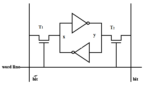
The diagram below is illustrate Static Random Access Memory (SRAM)Cell for the explanation. SRAM cell is make up of 2 inverters are cross-connected to form a latch .The latch is connected to 2 bit line by transistor T1 and T2 . T1 and T2 can switch opened or closed under control of word line.When word line is ground level, the transistors are turned off and the latch retrains its state. During the Read Operation ,Word line is activated to close switches T1 and T2 . If the cell is in state 1; the signal on b line is high and the signal on b’ line is low.The opposite is true if the cell is in state 0.Thus, b and b’ are always complements of each other’s. The sense /write circuit at the end of the two bit line monitors their state and sets the corresponding output accordingly. While in Write Operation ,the Sense/Write circuit drives bit lines b and b’, instead of sensing their state.It places the appropriate value on bit line b and its complement on b’ and activate the word
Oneplus 5T Flashing from Hydrogen OS to Oxygen OS
How to Convert Hydrogen OS to Oxygen OS in One plus 5T I just bought One Plus 5T, Is very easy but it will be hard if you did the wrong thing (that me ). I have done many mistakes from converting the Hydrogen os to Oxygen os. But I try to let you all avoid the mistake I have done. Ok, First download the Oxygen OS from the official website. (link: http://downloads.oneplus.net/devices/oneplus-5t/ ) (VERY VERY Important) After finishing download from the website. Open the PowerShell. (Win + R => Type in «Powershell» => Enter) Then try to locate the zip that you have just download. then type in the following in the PowerShell. Get-FileHash <filepath> -Algorithm MD5 (Replace the <filepath> with the file path of the zip you just download. Wait the result come out. The value must same as the value of md5 hash show on the website. If not same then redownload the rom. Then you need to create a ha