
The history of nanotechnology traces the development of the concepts and experimental work falling under the broad category of nanotechnology. Although nanotechnology is a relatively recent development in scientific research, the development of its central concepts happened over a longer period of time. The emergence of nanotechnology in the 1980s was caused by the convergence of experimental advances such as the invention of the scanning tunneling microscope in 1981 and the discovery of fullerenes in 1985, with the elucidation and popularization of a conceptual framework for the goals of nanotechnology beginning with the 1986 publication of the book Engines of Creation. The field was subject to growing public awareness and controversy in the early 2000s, with prominent debates about both its potential implications as well as the feasibility of the applications envisioned by advocates of molecular nanotechnology, and with governments moving to promote and fund research into nanotechnology. The early 2000s also saw the beginnings of commercial applications of nanotechnology, although these were limited to bulk applications of nanomaterials rather than the transformative applications envisioned by the field.
Early uses of nanomaterials[edit]
Carbon nanotubes have been found in pottery from Keeladi, India, dating to c. 600–300 BC, though it is not known how they formed or whether the substance containing them was employed deliberately.[1] Cementite nanowires have been observed in Damascus steel, a material dating back to c. 900 AD, their origin and means of manufacture also unknown.[2]
Although nanoparticles are associated with modern science, they were used by artisans as far back as the ninth century in Mesopotamia for creating a glittering effect on the surface of pots.[3][4]
In modern times, pottery from the Middle Ages and Renaissance often retains a distinct gold- or copper-colored metallic glitter. This luster is caused by a metallic film that was applied to the transparent surface of a glazing, which contains silver and copper nanoparticles dispersed homogeneously in the glassy matrix of the ceramic glaze. These nanoparticles are created by the artisans by adding copper and silver salts and oxides together with vinegar, ochre, and clay on the surface of previously-glazed pottery. The technique originated in the Muslim world. As Muslims were not allowed to use gold in artistic representations, they sought a way to create a similar effect without using real gold. The solution they found was using luster.[4][5]
Conceptual origins[edit]
Richard Feynman[edit]
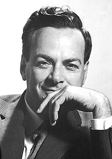
Richard Feynman gave a 1959 talk which many years later inspired the conceptual foundations of nanotechnology.
The American physicist Richard Feynman lectured, «There’s Plenty of Room at the Bottom,» at an American Physical Society meeting at Caltech on December 29, 1959, which is often held to have provided inspiration for the field of nanotechnology. Feynman had described a process by which the ability to manipulate individual atoms and molecules might be developed, using one set of precise tools to build and operate another proportionally smaller set, so on down to the needed scale. In the course of this, he noted, scaling issues would arise from the changing magnitude of various physical phenomena: gravity would become less important, surface tension and Van der Waals attraction would become more important.[6]
After Feynman’s death, a scholar studying the historical development of nanotechnology has concluded that his actual role in catalyzing nanotechnology research was limited, based on recollections from many of the people active in the nascent field in the 1980s and 1990s. Chris Toumey, a cultural anthropologist at the University of South Carolina, found that the published versions of Feynman’s talk had a negligible influence in the twenty years after it was first published, as measured by citations in the scientific literature, and not much more influence in the decade after the Scanning Tunneling Microscope was invented in 1981. Subsequently, interest in “Plenty of Room” in the scientific literature greatly increased in the early 1990s. This is probably because the term “nanotechnology” gained serious attention just before that time, following its use by K. Eric Drexler in his 1986 book, Engines of Creation: The Coming Era of Nanotechnology, which took the Feynman concept of a billion tiny factories and added the idea that they could make more copies of themselves via computer control instead of control by a human operator; and in a cover article headlined «Nanotechnology»,[7][8] published later that year in a mass-circulation science-oriented magazine, Omni. Toumey’s analysis also includes comments from distinguished scientists in nanotechnology who say that “Plenty of Room” did not influence their early work, and in fact most of them had not read it until a later date.[9][10]
These and other developments hint that the retroactive rediscovery of Feynman’s “Plenty of Room” gave nanotechnology a packaged history that provided an early date of December 1959, plus a connection to the charisma and genius of Richard Feynman. Feynman’s stature as a Nobel laureate and as an iconic figure in 20th century science surely helped advocates of nanotechnology and provided a valuable intellectual link to the past.[11]
Norio Taniguchi[edit]
The Japanese scientist called Norio Taniguchi of Tokyo University of Science was first to use the term «nano-technology» in a 1974 conference,[12] to describe semiconductor processes such as thin film deposition and ion beam milling exhibiting characteristic control on the order of a nanometer. His definition was, «‘Nano-technology’ mainly consists of the processing of, separation, consolidation, and deformation of materials by one atom or one molecule.» However, the term was not used again until 1981 when Eric Drexler, who was unaware of Taniguchi’s prior use of the term, published his first paper on nanotechnology in 1981.[13][14][15]
K. Eric Drexler[edit]

K. Eric Drexler developed and popularized the concept of nanotechnology and founded the field of molecular nanotechnology.
In the 1980s the idea of nanotechnology as a deterministic, rather than stochastic, handling of individual atoms and molecules was conceptually explored in depth by K. Eric Drexler, who promoted the technological significance of nano-scale phenomena and devices through speeches and two influential books.
In 1980, Drexler encountered Feynman’s provocative 1959 talk «There’s Plenty of Room at the Bottom» while preparing his initial scientific paper on the subject, “Molecular Engineering: An approach to the development of general capabilities for molecular manipulation,” published in the Proceedings of the National Academy of Sciences in 1981.[16] The term «nanotechnology» (which paralleled Taniguchi’s «nano-technology») was independently applied by Drexler in his 1986 book Engines of Creation: The Coming Era of Nanotechnology, which proposed the idea of a nanoscale «assembler» which would be able to build a copy of itself and of other items of arbitrary complexity. He also first published the term «grey goo» to describe what might happen if a hypothetical self-replicating machine, capable of independent operation, were constructed and released. Drexler’s vision of nanotechnology is often called «Molecular Nanotechnology» (MNT) or «molecular manufacturing.»
His 1991 Ph.D. work at the MIT Media Lab was the first doctoral degree on the topic of molecular nanotechnology and (after some editing) his thesis, «Molecular Machinery and Manufacturing with Applications to Computation,»[17] was published as Nanosystems: Molecular Machinery, Manufacturing, and Computation,[18] which received the Association of American Publishers award for Best Computer Science Book of 1992. Drexler founded the Foresight Institute in 1986 with the mission of «Preparing for nanotechnology.” Drexler is no longer a member of the Foresight Institute.[citation needed]
Experimental research and advances[edit]
In nanoelectronics, nanoscale thickness was demonstrated in the gate oxide and thin films used in transistors as early as the 1960s, but it was not until the late 1990s that MOSFETs (metal–oxide–semiconductor field-effect transistors) with nanoscale gate length were demonstrated. Nanotechnology and nanoscience got a boost in the early 1980s with two major developments: the birth of cluster science and the invention of the scanning tunneling microscope (STM). These developments led to the discovery of fullerenes in 1985 and the structural assignment of carbon nanotubes in 1991. The development of FinFET in the 1990s aldo laid the foundations for modern nanoelectronic semiconductor device fabrication.
Invention of scanning probe microscopy[edit]


Gerd Binnig (left) and Heinrich Rohrer (right) won the 1986 Nobel Prize in Physics for their 1981 invention of the scanning tunneling microscope.
The scanning tunneling microscope, an instrument for imaging surfaces at the atomic level, was developed in 1981 by Gerd Binnig and Heinrich Rohrer at IBM Zurich Research Laboratory, for which they were awarded the Nobel Prize in Physics in 1986.[19][20] Binnig, Calvin Quate and Christoph Gerber invented the first atomic force microscope in 1986. The first commercially available atomic force microscope was introduced in 1989.
IBM researcher Don Eigler was the first to manipulate atoms using a scanning tunneling microscope in 1989. He used 35 Xenon atoms to spell out the IBM logo.[21] He shared the 2010 Kavli Prize in Nanoscience for this work.[22]
Advances in interface and colloid science[edit]
Interface and colloid science had existed for nearly a century before they became associated with nanotechnology.[23][24] The first observations and size measurements of nanoparticles had been made during the first decade of the 20th century by Richard Adolf Zsigmondy, winner of the 1925 Nobel Prize in Chemistry, who made a detailed study of gold sols and other nanomaterials with sizes down to 10 nm using an ultramicroscope which was capable of visualizing particles much smaller than the light wavelength.[25] Zsigmondy was also the first to use the term «nanometer» explicitly for characterizing particle size. In the 1920s, Irving Langmuir, winner of the 1932 Nobel Prize in Chemistry, and Katharine B. Blodgett introduced the concept of a monolayer, a layer of material one molecule thick. In the early 1950s, Derjaguin and Abrikosova conducted the first measurement of surface forces.[26]
In 1974 the process of atomic layer deposition for depositing uniform thin films one atomic layer at a time was developed and patented by Tuomo Suntola and co-workers in Finland.[27]
In another development, the synthesis and properties of semiconductor nanocrystals were studied. This led to a fast increasing number of semiconductor nanoparticles of quantum dots.
Discovery of fullerenes[edit]


Harry Kroto (left) won the 1996 Nobel Prize in Chemistry along with Richard Smalley (pictured below) and Robert Curl for their 1985 discovery of buckminsterfullerene, while Sumio Iijima (right) won the inaugural 2008 Kavli Prize in Nanoscience for his 1991 discovery of carbon nanotubes.
Fullerenes were discovered in 1985 by Harry Kroto, Richard Smalley, and Robert Curl, who together won the 1996 Nobel Prize in Chemistry. Smalley’s research in physical chemistry investigated formation of inorganic and semiconductor clusters using pulsed molecular beams and time of flight mass spectrometry. As a consequence of this expertise, Curl introduced him to Kroto in order to investigate a question about the constituents of astronomical dust. These are carbon rich grains expelled by old stars such as R Corona Borealis. The result of this collaboration was the discovery of C60 and the fullerenes as the third allotropic form of carbon. Subsequent discoveries included the endohedral fullerenes, and the larger family of fullerenes the following year.[28][29]
The discovery of carbon nanotubes is largely attributed to Sumio Iijima of NEC in 1991, although carbon nanotubes have been produced and observed under a variety of conditions prior to 1991.[30] Iijima’s discovery of multi-walled carbon nanotubes in the insoluble material of arc-burned graphite rods in 1991[31] and Mintmire, Dunlap, and White’s independent prediction that if single-walled carbon nanotubes could be made, then they would exhibit remarkable conducting properties[32] helped create the initial buzz that is now associated with carbon nanotubes. Nanotube research accelerated greatly following the independent discoveries[33][34] by Bethune at IBM[35] and Iijima at NEC of single-walled carbon nanotubes and methods to specifically produce them by adding transition-metal catalysts to the carbon in an arc discharge.
In the early 1990s Huffman and Kraetschmer, of the University of Arizona, discovered how to synthesize and purify large quantities of fullerenes. This opened the door to their characterization and functionalization by hundreds of investigators in government and industrial laboratories. Shortly after, rubidium doped C60 was found to be a mid temperature (Tc = 32 K) superconductor. At a meeting of the Materials Research Society in 1992, Dr. T. Ebbesen (NEC) described to a spellbound audience his discovery and characterization of carbon nanotubes. This event sent those in attendance and others downwind of his presentation into their laboratories to reproduce and push those discoveries forward. Using the same or similar tools as those used by Huffman and Kratschmer, hundreds of researchers further developed the field of nanotube-based nanotechnology.
Government and corporate support[edit]
National Nanotechnology Initiative[edit]

The National Nanotechnology Initiative is a United States federal nanotechnology research and development program. “The NNI serves as the central point of communication, cooperation, and collaboration for all Federal agencies engaged in nanotechnology research, bringing together the expertise needed to advance this broad and complex field.»[36] Its goals are to advance a world-class nanotechnology research and development (R&D) program, foster the transfer of new technologies into products for commercial and public benefit, develop and sustain educational resources, a skilled workforce, and the supporting infrastructure and tools to advance nanotechnology, and support responsible development of nanotechnology. The initiative was spearheaded by Mihail Roco, who formally proposed the National Nanotechnology Initiative to the Office of Science and Technology Policy during the Clinton administration in 1999, and was a key architect in its development. He is currently the Senior Advisor for Nanotechnology at the National Science Foundation, as well as the founding chair of the National Science and Technology Council subcommittee on Nanoscale Science, Engineering and Technology.[37]
President Bill Clinton advocated nanotechnology development. In a 21 January 2000 speech[38] at the California Institute of Technology, Clinton said, «Some of our research goals may take twenty or more years to achieve, but that is precisely why there is an important role for the federal government.» Feynman’s stature and concept of atomically precise fabrication played a role in securing funding for nanotechnology research, as mentioned in President Clinton’s speech:
My budget supports a major new National Nanotechnology Initiative, worth $500 million. Caltech is no stranger to the idea of nanotechnology the ability to manipulate matter at the atomic and molecular level. Over 40 years ago, Caltech’s own Richard Feynman asked, «What would happen if we could arrange the atoms one by one the way we want them?»[39]
President George W. Bush further increased funding for nanotechnology. On December 3, 2003 Bush signed into law the 21st Century Nanotechnology Research and Development Act,[40] which authorizes expenditures for five of the participating agencies totaling US$3.63 billion over four years.[41] The NNI budget supplement for Fiscal Year 2009 provides $1.5 billion to the NNI, reflecting steady growth in the nanotechnology investment.[42]
Growing public awareness and controversy[edit]
«Why the future doesn’t need us»[edit]
«Why the future doesn’t need us» is an article written by Bill Joy, then Chief Scientist at Sun Microsystems, in the April 2000 issue of Wired magazine. In the article, he argues that «Our most powerful 21st-century technologies — robotics, genetic engineering, and nanotech — are threatening to make humans an endangered species.» Joy argues that developing technologies provide a much greater danger to humanity than any technology before it has ever presented. In particular, he focuses on genetics, nanotechnology and robotics. He argues that 20th-century technologies of destruction, such as the nuclear bomb, were limited to large governments, due to the complexity and cost of such devices, as well as the difficulty in acquiring the required materials. He also voices concern about increasing computer power. His worry is that computers will eventually become more intelligent than we are, leading to such dystopian scenarios as robot rebellion. He notably quotes the Unabomber on this topic. After the publication of the article, Bill Joy suggested assessing technologies to gauge their implicit dangers, as well as having scientists refuse to work on technologies that have the potential to cause harm.
In the AAAS Science and Technology Policy Yearbook 2001 article titled A Response to Bill Joy and the Doom-and-Gloom Technofuturists, Bill Joy was criticized for having technological tunnel vision on his prediction, by failing to consider social factors.[43] In Ray Kurzweil’s The Singularity Is Near, he questioned the regulation of potentially dangerous technology, asking «Should we tell the millions of people afflicted with cancer and other devastating conditions that we are canceling the development of all bioengineered treatments because there is a risk that these same technologies may someday be used for malevolent purposes?».
Prey[edit]
Prey is a 2002 novel by Michael Crichton which features an artificial swarm of nanorobots which develop intelligence and threaten their human inventors. The novel generated concern within the nanotechnology community that the novel could negatively affect public perception of nanotechnology by creating fear of a similar scenario in real life.[44]
Drexler–Smalley debate[edit]
Richard Smalley, best known for co-discovering the soccer ball-shaped “buckyball” molecule and a leading advocate of nanotechnology and its many applications, was an outspoken critic of the idea of molecular assemblers, as advocated by Eric Drexler. In 2001 he introduced scientific objections to them[45] attacking the notion of universal assemblers in a 2001 Scientific American article, leading to a rebuttal later that year from Drexler and colleagues,[46] and eventually to an exchange of open letters in 2003.[47]
Smalley criticized Drexler’s work on nanotechnology as naive, arguing that chemistry is extremely complicated, reactions are hard to control, and that a universal assembler is science fiction. Smalley believed that such assemblers were not physically possible and introduced scientific objections to them. His two principal technical objections, which he had termed the “fat fingers problem» and the «sticky fingers problem”, argued against the feasibility of molecular assemblers being able to precisely select and place individual atoms. He also believed that Drexler’s speculations about apocalyptic dangers of molecular assemblers threaten the public support for development of nanotechnology.
Smalley first argued that «fat fingers» made MNT impossible. He later argued that nanomachines would have to resemble chemical enzymes more than Drexler’s assemblers and could only work in water. He believed these would exclude the possibility of «molecular assemblers» that worked by precision picking and placing of individual atoms. Also, Smalley argued that nearly all of modern chemistry involves reactions that take place in a solvent (usually water), because the small molecules of a solvent contribute many things, such as lowering binding energies for transition states. Since nearly all known chemistry requires a solvent, Smalley felt that Drexler’s proposal to use a high vacuum environment was not feasible.
Smalley also believed that Drexler’s speculations about apocalyptic dangers of self-replicating machines that have been equated with «molecular assemblers» would threaten the public support for development of nanotechnology. To address the debate between Drexler and Smalley regarding molecular assemblers Chemical & Engineering News published a point-counterpoint consisting of an exchange of letters that addressed the issues.[47]
Drexler and coworkers responded to these two issues[46] in a 2001 publication. Drexler and colleagues noted that Drexler never proposed universal assemblers able to make absolutely anything, but instead proposed more limited assemblers able to make a very wide variety of things. They challenged the relevance of Smalley’s arguments to the more specific proposals advanced in Nanosystems. Drexler maintained that both were straw man arguments, and in the case of enzymes, Prof. Klibanov wrote in 1994, «…using an enzyme in organic solvents eliminates several obstacles…»[48] Drexler also addresses this in Nanosystems by showing mathematically that well designed catalysts can provide the effects of a solvent and can fundamentally be made even more efficient than a solvent/enzyme reaction could ever be. Drexler had difficulty in getting Smalley to respond, but in December 2003, Chemical & Engineering News carried a 4-part debate.[47]
Ray Kurzweil spends four pages in his book ‘The Singularity Is Near’ to showing that Richard Smalley’s arguments are not valid, and disputing them point by point. Kurzweil ends by stating that Drexler’s visions are very practicable and even happening already.[49]
Royal Society report on the implications of nanotechnology[edit]
The Royal Society and Royal Academy of Engineering’s 2004 report on the implications of nanoscience and nanotechnologies[50] was inspired by Prince Charles’ concerns about nanotechnology, including molecular manufacturing. However, the report spent almost no time on molecular manufacturing.[51] In fact, the word «Drexler» appears only once in the body of the report (in passing), and «molecular manufacturing» or «molecular nanotechnology» not at all. The report covers various risks of nanoscale technologies, such as nanoparticle toxicology. It also provides a useful overview of several nanoscale fields. The report contains an annex (appendix) on grey goo, which cites a weaker variation of Richard Smalley’s contested argument against molecular manufacturing. It concludes that there is no evidence that autonomous, self replicating nanomachines will be developed in the foreseeable future, and suggests that regulators should be more concerned with issues of nanoparticle toxicology.
Initial commercial applications[edit]
The early 2000s saw the beginnings of the use of nanotechnology in commercial products, although most applications are limited to the bulk use of passive nanomaterials. Examples include titanium dioxide and zinc oxide nanoparticles in sunscreen, cosmetics and some food products; silver nanoparticles in food packaging, clothing, disinfectants and household appliances such as Silver Nano; carbon nanotubes for stain-resistant textiles; and cerium oxide as a fuel catalyst.[52] As of March 10, 2011, the Project on Emerging Nanotechnologies estimated that over 1300 manufacturer-identified nanotech products are publicly available, with new ones hitting the market at a pace of 3–4 per week.[53]
The National Science Foundation funded researcher David Berube to study the field of nanotechnology[when?]. His findings are published in the monograph Nano-Hype: The Truth Behind the Nanotechnology Buzz. This study concludes that much of what is sold as “nanotechnology” is in fact a recasting of straightforward materials science, which is leading to a “nanotech industry built solely on selling nanotubes, nanowires, and the like” which will “end up with a few suppliers selling low margin products in huge volumes.» Further applications which require actual manipulation or arrangement of nanoscale components await further research. Though technologies branded with the term ‘nano’ are sometimes little related to and fall far short of the most ambitious and transformative technological goals of the sort in molecular manufacturing proposals, the term still connotes such ideas. According to Berube, there may be a danger that a «nano bubble» will form, or is forming already, from the use of the term by scientists and entrepreneurs to garner funding, regardless of interest in the transformative possibilities of more ambitious and far-sighted work.[54]
Invention of ionizable cationic lipids at the turn of the 21st century allowed subsequent development of solid lipid nanoparticles, which in the 2020s became the most successful and well-known non-viral nanoparticle drug delivery system due to their use in several mRNA vaccines during the COVID-19 pandemic.
See also[edit]
- Timeline of carbon nanotubes
- Discovery of graphene
- History of DNA nanotechnology
References[edit]
- ^ Kokarneswaran, M., Selvaraj, P., Ashokan, T., Mohan, N., Chadrasekaran V (2020). «Discovery of carbon nanotubes in sixth century BC potteries from Keeladi, India». Scientific Reports. 10 (1): 19786. Bibcode:2020NatSR..1019786K. doi:10.1038/s41598-020-76720-z. PMC 7666134. PMID 33188244.
{{cite journal}}: CS1 maint: multiple names: authors list (link) - ^ Sanderson, Katharine (2006-11-15). «Sharpest cut from nanotube sword». Nature News: news061113–11. doi:10.1038/news061113-11. S2CID 136774602.
- ^ Reiss, Gunter; Hutten, Andreas (2010). «Magnetic Nanoparticles». In Sattler, Klaus D. (ed.). Handbook of Nanophysics: Nanoparticles and Quantum Dots. CRC Press. pp. 2–1. ISBN 9781420075458.
- ^ a b Khan, Firdos Alam (2012). Biotechnology Fundamentals. CRC Press. p. 328. ISBN 9781439820094.
- ^ Rawson, Philip S. (1984). Ceramics. University of Pennsylvania Press. ISBN 978-0-8122-1156-6.
- ^ Gribbin, John; Gribbin, Mary (1997). Richard Feynman: A Life in Science. Dutton. p. 170. ISBN 978-0-452-27631-4.
- ^ Hapgood, Fred (November 1986). ««Nanotechnology» / «Tinytech»«. Omni: 56.
- ^ Drexler, Eric (15 December 2009). «The promise that launched the field of nanotechnology». Metamodern: The Trajectory of Technology. Archived from the original on 14 July 2011. Retrieved 13 May 2011.
- ^ Toumey, Chris (2005). «Apostolic Succession» (PDF). Engineering & Science. 1/2: 16–23.
- ^ Toumey, Chris (2008). «Reading Feynman into Nanotechnology: A Text for a New Science» (PDF). Techné. 13 (3): 133–168. Archived from the original (PDF) on 2009-09-19.
- ^ Milburn, Colin (2008). Nanovision: Engineering the Future. Duke University Press. ISBN 978-0-8223-4265-6.
- ^ Taniguchi, Norio (1974). «On the Basic Concept of ‘Nano-Technology’«. Proceedings of the International Conference on Production Engineering, Tokyo, 1974, Part II.
- ^ Bassett, Deborah R. (2010). «Taniguchi, Norio». In Guston, David H. (ed.). Encyclopedia of nanoscience and society. London: SAGE. p. 747. ISBN 9781452266176. Retrieved 3 August 2014.
- ^ Koodali, Ranjit T.; Klabunde, Kenneth J. (2012). «Nanotechnology: Fandamental Principles and Applications». In Kent, James A. (ed.). Handbook of industrial chemistry and biotechnology, volume 1 (12th ed.). New York: Springer. p. 250. ISBN 9781461442592. Retrieved 3 August 2014.
- ^ Maynard, edited by Graeme A. Hodge, Diana M. Bowman, Andrew D. (2010). «Tracing and disputing the story of nanotechnology». In Hodge, Graeme A.; Bowman, Diana M.; Maynard, Andrew D. (eds.). International handbook on regulating nanotechnologies. Cheltenham, UK: Edward Elgar. p. 54. ISBN 9781849808125. Retrieved 4 August 2014.
- ^ Drexler, K. E. (1981). «Molecular engineering: An approach to the development of general capabilities for molecular manipulation». Proceedings of the National Academy of Sciences of the United States of America. 78 (9): 5275–5278. Bibcode:1981PNAS…78.5275D. doi:10.1073/pnas.78.9.5275. PMC 348724. PMID 16593078.
- ^ Drexler, K. Eric. Molecular Machinery and Manufacturing with Applications to Computation (PDF) (Ph.D. thesis). Massachusetts Institute of Technology. Archived from the original (PDF) on 2008-09-08.
- ^ Drexler, K. Eric (1992). Nanosystems: Molecular Machinery, Manufacturing, and Computation. Wiley. ISBN 978-0-471-57518-4. Retrieved 14 May 2011.
- ^ Binnig, G.; Rohrer, H. (1986). «Scanning tunneling microscopy». IBM Journal of Research and Development. 30 (4): 355–69.
- ^ «Press Release: the 1996 Nobel Prize in Physics». Nobelprize.org. 15 October 1986. Retrieved 12 May 2011.
- ^ Shankland, Stephen (28 September 2009). «IBM’s 35 atoms and the rise of nanotech». CNET. Retrieved 12 May 2011.
- ^ «The Kavli Prize Laureates 2010». The Norwegian Academy of Science and Letters. Archived from the original on 12 May 2011. Retrieved 13 May 2011.
- ^ Efremov, I.F. (1976). «Periodic Colloidal Structures». In Matijevic, E. (ed.). Surface and Colloid Science. Vol. 8. New York: Wiley.
- ^ Lyklema, J. (2000). Fundamentals of Interface and Colloid Science. Academic Press. ISBN 978-0-12-460523-7. Archived from the original on 2012-10-12. Retrieved 2011-05-12.
- ^ Zsigmondy, R. (1914). Colloids and the Ultramicroscope. New York: J.Wiley and Sons. Retrieved 10 May 2011.
- ^ Derjaguin, B. V.; Titijevskaia, A. S.; Abricossova, I. I.; Malkina, A. D. (1954). «Investigations of the forces of interaction of surfaces in different media and their application to the problem of colloid stability». Discussions of the Faraday Society. 18: 24. doi:10.1039/DF9541800024.
- ^ «History of Atomic Layer Deposition». Finnish Micro & Nano Technology Network. Archived from the original on 28 September 2007.
- ^ Kroto, H. W.; Heath, J. R.; O’Brien, S. C.; Curl, R. F.; Smalley, R. E. (1985). «C60: Buckminsterfullerene». Nature. 318 (6042): 162–163. Bibcode:1985Natur.318..162K. doi:10.1038/318162a0. S2CID 4314237.
- ^ Adams, W Wade; Baughman, Ray H (2005). «Retrospective: Richard E. Smalley (1943–2005)». Science. Vol. 310, no. 5756 (published Dec 23, 2005). p. 1916. doi:10.1126/science.1122120. PMID 16373566.
- ^ Monthioux, Marc; Kuznetsov, V (2006). «Who should be given the credit for the discovery of carbon nanotubes?» (PDF). Carbon. 44 (9): 1621–1623. doi:10.1016/j.carbon.2006.03.019.
- ^ Iijima, Sumio (7 November 1991). «Helical microtubules of graphitic carbon». Nature. 354 (6348): 56–58. Bibcode:1991Natur.354…56I. doi:10.1038/354056a0. S2CID 4302490.
- ^ Mintmire, J.W.; Dunlap, BI; White, CT (1992). «Are Fullerene Tubules Metallic?». Physical Review Letters. 68 (5): 631–634. Bibcode:1992PhRvL..68..631M. doi:10.1103/PhysRevLett.68.631. PMID 10045950.
- ^ Bethune, D. S.; Klang, C. H.; De Vries, M. S.; Gorman, G.; Savoy, R.; Vazquez, J.; Beyers, R. (1993). «Cobalt-catalyzed growth of carbon nanotubes with single-atomic-layer walls». Nature. 363 (6430): 605–607. Bibcode:1993Natur.363..605B. doi:10.1038/363605a0. S2CID 4321984.
- ^ Iijima, Sumio; Ichihashi, Toshinari (1993). «Single-shell carbon nanotubes of 1-nm diameter». Nature. 363 (6430): 603–605. Bibcode:1993Natur.363..603I. doi:10.1038/363603a0. S2CID 4314177.
- ^ «The Discovery of Single-Wall Carbon Nanotubes at IBM». IBM. 2016-07-25.
- ^ «About the NNI | Nano».
- ^
«Dr. Mihail C. Roco, Senior Advisor for Nanotechnology, National Science Foundation». National Science Foundation. Archived from the original on 11 April 2010. Retrieved 8 November 2009. - ^ «President Clinton’s Address to Caltech on Science and Technology». California Institute of Technology. Archived from the original on 7 August 2011. Retrieved 13 May 2011.
- ^ Jones, Richard M. (21 January 2000). «President Requests Significant Increase in FY 2001 Research Budget». FYI: The AIP Bulletin of Science Policy News. American Institute of Physics. Retrieved 13 May 2011.
- ^ «21st Century Nanotechnology Research and Development Act (Public Law 108-153)». United States Government Printing Office. Retrieved 12 May 2011.
- ^ «Remarks Prepared for Delivery: National Nanotechnology Initiative Conference, Senator George Allen, Thursday, April 1, 2004». United States National Nanotechnology Initiative. Archived from the original on 27 September 2007.
- ^ «National Nanotechnology Initiative: FY 2009 Budget & Highlights» (PDF). United States National Nanotechnology Initiative. Archived from the original (PDF) on 27 May 2010.
- ^ Brown, John Seely and Duguid, Paul (13 April 2000). «A Response to Bill Joy and the Doom-and-Gloom Technofuturists» (PDF). Archived from the original (PDF) on 31 December 2003. Retrieved 12 May 2011.
{{cite web}}: CS1 maint: multiple names: authors list (link) - ^ Edwards, Steven A. (2006). The Nanotech Pioneers: Where Are They Taking Us?. Weinheim: Wiley-VCH. pp. 22–23.
- ^ Smalley, Richard E. (September 2001). «Of Chemistry, Love and Nanobots». Scientific American. 285 (3): 76–7. Bibcode:2001SciAm.285c..76S. doi:10.1038/scientificamerican0901-76. PMID 11524973. Archived from the original on 2012-07-23. Retrieved 2011-05-12.
- ^ a b Drexler, K. Eric; Forrest, David; Freitas, Robert A.; Hall, J. Storrs; Jacobstein, Neil; McKendree, Tom; Merkle, Ralph; Peterson, Christine (2001). «Debate About Assemblers — Smalley Rebuttal». Institute for Molecular Manufacturing. Retrieved 9 May 2010.
- ^ a b c «Nanotechnology: Drexler and Smalley make the case for and against ‘molecular assemblers’«. Chemical & Engineering News. 81 (48): 37–42. 1 December 2003. doi:10.1021/cen-v081n036.p037. Retrieved 9 May 2010.
- ^ Phoenix, Chris (December 2003). «Of Chemistry, Nanobots, and Policy». Center for Responsible Nanotechnology. Retrieved 12 May 2011.
- ^ Kurzweil, Ray (2005). The Singularity Is Near. pp. 193–196. ISBN 978-0-670-03384-3.
- ^ «Nanoscience and nanotechnologies: opportunities and uncertainties». Royal Society and Royal Academy of Engineering. July 2004. Archived from the original on 3 July 2018. Retrieved 13 May 2011.
- ^ «Royal Society in Denial». Center for Responsible Nanotechnology. 31 July 2004. Retrieved 13 May 2011.
- ^ «Nanotechnology Information Center: Properties, Applications, Research, and Safety Guidelines». American Elements. Retrieved 13 May 2011.
- ^ «Analysis: This is the first publicly available on-line inventory of nanotechnology-based consumer products». The Project on Emerging Nanotechnologies. 2008. Retrieved 13 May 2011.
- ^ Berube, David (2006). Nano-Hype: The Truth Behind the Nanotechnology Buzz. Amherst, NY: Prometheus Books. Archived from the original on 2017-10-28. Retrieved 2020-01-15.
External links[edit]
- T. Mappes; et al. (2012). «The Invention of Immersion Ultramicroscopy in 1912—The Birth of Nanotechnology?». Angewandte Chemie International Edition. 51 (45): 11208–11212. doi:10.1002/anie.201204688. PMID 23065955.
- Who Invented Nanotechnology
- What is Nanotechnology with Full Information
- How to make a career in technology
Nanotechnology, often shortened to nanotech, is the use of matter on atomic, molecular, and supramolecular scales for industrial purposes. The earliest, widespread description of nanotechnology referred to the particular technological goal of precisely manipulating atoms and molecules for fabrication of macroscale products, also now referred to as molecular nanotechnology.[1][2] A more generalized description of nanotechnology was subsequently established by the National Nanotechnology Initiative, which defined nanotechnology as the manipulation of matter with at least one dimension sized from 1 to 100 nanometers (nm). This definition reflects the fact that quantum mechanical effects are important at this quantum-realm scale, and so the definition shifted from a particular technological goal to a research category inclusive of all types of research and technologies that deal with the special properties of matter which occur below the given size threshold. It is therefore common to see the plural form «nanotechnologies» as well as «nanoscale technologies» to refer to the broad range of research and applications whose common trait is size.

Nanotechnology as defined by size is naturally broad, including fields of science as diverse as surface science, organic chemistry, molecular biology, semiconductor physics, energy storage,[3][4] engineering,[5] microfabrication,[6] and molecular engineering.[7] The associated research and applications are equally diverse, ranging from extensions of conventional device physics to completely new approaches based upon molecular self-assembly,[8] from developing new materials with dimensions on the nanoscale to direct control of matter on the atomic scale.
Scientists currently debate the future implications of nanotechnology. Nanotechnology may be able to create many new materials and devices with a vast range of applications, such as in nanomedicine, nanoelectronics, biomaterials energy production, and consumer products. On the other hand, nanotechnology raises many of the same issues as any new technology, including concerns about the toxicity and environmental impact of nanomaterials,[9] and their potential effects on global economics, as well as speculation about various doomsday scenarios. These concerns have led to a debate among advocacy groups and governments on whether special regulation of nanotechnology is warranted.
Origins
The concepts that seeded nanotechnology were first discussed in 1959 by renowned physicist Richard Feynman in his talk There’s Plenty of Room at the Bottom, in which he described the possibility of synthesis via direct manipulation of atoms.
Comparison of Nanomaterials Sizes
The term «nano-technology» was first used by Norio Taniguchi in 1974, though it was not widely known. Inspired by Feynman’s concepts, K. Eric Drexler used the term «nanotechnology» in his 1986 book Engines of Creation: The Coming Era of Nanotechnology, which proposed the idea of a nanoscale «assembler» which would be able to build a copy of itself and of other items of arbitrary complexity with atomic control. Also in 1986, Drexler co-founded The Foresight Institute (with which he is no longer affiliated) to help increase public awareness and understanding of nanotechnology concepts and implications.
The emergence of nanotechnology as a field in the 1980s occurred through convergence of Drexler’s theoretical and public work, which developed and popularized a conceptual framework for nanotechnology, and high-visibility experimental advances that drew additional wide-scale attention to the prospects of atomic control of matter. In the 1980s, two major breakthroughs sparked the growth of nanotechnology in the modern era. First, the invention of the scanning tunneling microscope in 1981 which provided unprecedented visualization of individual atoms and bonds, and was successfully used to manipulate individual atoms in 1989. The microscope’s developers Gerd Binnig and Heinrich Rohrer at IBM Zurich Research Laboratory received a Nobel Prize in Physics in 1986.[10][11] Binnig, Quate and Gerber also invented the analogous atomic force microscope that year.
Buckminsterfullerene C60, also known as the buckyball, is a representative member of the carbon structures known as fullerenes. Members of the fullerene family are a major subject of research falling under the nanotechnology umbrella.
Second, fullerenes were discovered in 1985 by Harry Kroto, Richard Smalley, and Robert Curl, who together won the 1996 Nobel Prize in Chemistry.[12][13] C60 was not initially described as nanotechnology; the term was used regarding subsequent work with related carbon nanotubes (sometimes called graphene tubes or Bucky tubes) which suggested potential applications for nanoscale electronics and devices. The discovery of carbon nanotubes is largely attributed to Sumio Iijima of NEC in 1991,[14] for which Iijima won the inaugural 2008 Kavli Prize in Nanoscience.
In the early 2000s, the field garnered increased scientific, political, and commercial attention that led to both controversy and progress. Controversies emerged regarding the definitions and potential implications of nanotechnologies, exemplified by the Royal Society’s report on nanotechnology.[15] Challenges were raised regarding the feasibility of applications envisioned by advocates of molecular nanotechnology, which culminated in a public debate between Drexler and Smalley in 2001 and 2003.[16]
Meanwhile, commercialization of products based on advancements in nanoscale technologies began emerging. These products are limited to bulk applications of nanomaterials and do not involve atomic control of matter. Some examples include the Silver Nano platform for using silver nanoparticles as an antibacterial agent, nanoparticle-based transparent sunscreens, carbon fiber strengthening using silica nanoparticles, and carbon nanotubes for stain-resistant textiles.[17][18]
Governments moved to promote and fund research into nanotechnology, such as in the U.S. with the National Nanotechnology Initiative, which formalized a size-based definition of nanotechnology and established funding for research on the nanoscale, and in Europe via the European Framework Programmes for Research and Technological Development.
By the mid-2000s new and serious scientific attention began to flourish. Projects emerged to produce nanotechnology roadmaps[19][20] which center on atomically precise manipulation of matter and discuss existing and projected capabilities, goals, and applications.
Fundamental concepts
Nanotechnology is the engineering of functional systems at the molecular scale. This covers both current work and concepts that are more advanced. In its original sense, nanotechnology refers to the projected ability to construct items from the bottom up, using techniques and tools being developed today to make complete, high-performance products.
One nanometer (nm) is one billionth, or 10−9, of a meter. By comparison, typical carbon-carbon bond lengths, or the spacing between these atoms in a molecule, are in the range 0.12–0.15 nm, and a DNA double-helix has a diameter around 2 nm. On the other hand, the smallest cellular life-forms, the bacteria of the genus Mycoplasma, are around 200 nm in length. By convention, nanotechnology is taken as the scale range 1 to 100 nm following the definition used by the National Nanotechnology Initiative in the US. The lower limit is set by the size of atoms (hydrogen has the smallest atoms, which are approximately a quarter of a nm kinetic diameter) since nanotechnology must build its devices from atoms and molecules. The upper limit is more or less arbitrary but is around the size below which the phenomena not observed in larger structures start to become apparent and can be made use of in the nano device.[21] These new phenomena make nanotechnology distinct from devices which are merely miniaturised versions of an equivalent macroscopic device; such devices are on a larger scale and come under the description of microtechnology.[22]
To put that scale in another context, the comparative size of a nanometer to a meter is the same as that of a marble to the size of the earth.[23] Or another way of putting it: a nanometer is the amount an average man’s beard grows in the time it takes him to raise the razor to his face.[23]
Two main approaches are used in nanotechnology. In the «bottom-up» approach, materials and devices are built from molecular components which assemble themselves chemically by principles of molecular recognition.[24] In the «top-down» approach, nano-objects are constructed from larger entities without atomic-level control.[25]
Areas of physics such as nanoelectronics, nanomechanics, nanophotonics and nanoionics have evolved during the last few decades to provide a basic scientific foundation of nanotechnology.
Larger to smaller: a materials perspective
Several phenomena become pronounced as the size of the system decreases. These include statistical mechanical effects, as well as quantum mechanical effects, for example the «quantum size effect» where the electronic properties of solids are altered with great reductions in particle size. This effect does not come into play by going from macro to micro dimensions. However, quantum effects can become significant when the nanometer size range is reached, typically at distances of 100 nanometers or less, the so-called quantum realm. Additionally, a number of physical (mechanical, electrical, optical, etc.) properties change when compared to macroscopic systems. One example is the increase in surface area to volume ratio altering mechanical, thermal and catalytic properties of materials. Diffusion and reactions at nanoscale, nanostructures materials and nanodevices with fast ion transport are generally referred to nanoionics. Mechanical properties of nanosystems are of interest in the nanomechanics research. The catalytic activity of nanomaterials also opens potential risks in their interaction with biomaterials.
Materials reduced to the nanoscale can show different properties compared to what they exhibit on a macroscale, enabling unique applications. For instance, opaque substances can become transparent (copper); stable materials can turn combustible (aluminium); insoluble materials may become soluble (gold). A material such as gold, which is chemically inert at normal scales, can serve as a potent chemical catalyst at nanoscales. Much of the fascination with nanotechnology stems from these quantum and surface phenomena that matter exhibits at the nanoscale.[26]
Simple to complex: a molecular perspective
Modern synthetic chemistry has reached the point where it is possible to prepare small molecules to almost any structure. These methods are used today to manufacture a wide variety of useful chemicals such as pharmaceuticals or commercial polymers. This ability raises the question of extending this kind of control to the next-larger level, seeking methods to assemble these single molecules into supramolecular assemblies consisting of many molecules arranged in a well defined manner.
These approaches utilize the concepts of molecular self-assembly and/or supramolecular chemistry to automatically arrange themselves into some useful conformation through a bottom-up approach. The concept of molecular recognition is especially important: molecules can be designed so that a specific configuration or arrangement is favored due to non-covalent intermolecular forces. The Watson–Crick basepairing rules are a direct result of this, as is the specificity of an enzyme being targeted to a single substrate, or the specific folding of the protein itself. Thus, two or more components can be designed to be complementary and mutually attractive so that they make a more complex and useful whole.
Such bottom-up approaches should be capable of producing devices in parallel and be much cheaper than top-down methods, but could potentially be overwhelmed as the size and complexity of the desired assembly increases. Most useful structures require complex and thermodynamically unlikely arrangements of atoms. Nevertheless, there are many examples of self-assembly based on molecular recognition in biology, most notably Watson–Crick basepairing and enzyme-substrate interactions. The challenge for nanotechnology is whether these principles can be used to engineer new constructs in addition to natural ones.
Molecular nanotechnology: a long-term view
Molecular nanotechnology, sometimes called molecular manufacturing, describes engineered nanosystems (nanoscale machines) operating on the molecular scale. Molecular nanotechnology is especially associated with the molecular assembler, a machine that can produce a desired structure or device atom-by-atom using the principles of mechanosynthesis. Manufacturing in the context of productive nanosystems is not related to, and should be clearly distinguished from, the conventional technologies used to manufacture nanomaterials such as carbon nanotubes and nanoparticles.
When the term «nanotechnology» was independently coined and popularized by Eric Drexler (who at the time was unaware of an earlier usage by Norio Taniguchi) it referred to a future manufacturing technology based on molecular machine systems. The premise was that molecular-scale biological analogies of traditional machine components demonstrated molecular machines were possible: by the countless examples found in biology, it is known that sophisticated, stochastically optimized biological machines can be produced.
It is hoped that developments in nanotechnology will make possible their construction by some other means, perhaps using biomimetic principles. However, Drexler and other researchers[27] have proposed that advanced nanotechnology, although perhaps initially implemented by biomimetic means, ultimately could be based on mechanical engineering principles, namely, a manufacturing technology based on the mechanical functionality of these components (such as gears, bearings, motors, and structural members) that would enable programmable, positional assembly to atomic specification.[28] The physics and engineering performance of exemplar designs were analyzed in Drexler’s book Nanosystems: Molecular Machinery, Manufacturing, and Computation.[2]
In general it is very difficult to assemble devices on the atomic scale, as one has to position atoms on other atoms of comparable size and stickiness. Another view, put forth by Carlo Montemagno,[29] is that future nanosystems will be hybrids of silicon technology and biological molecular machines. Richard Smalley argued that mechanosynthesis are impossible due to the difficulties in mechanically manipulating individual molecules.
This led to an exchange of letters in the ACS publication Chemical & Engineering News in 2003.[30] Though biology clearly demonstrates that molecular machine systems are possible, non-biological molecular machines are today only in their infancy. Leaders in research on non-biological molecular machines are Dr. Alex Zettl and his colleagues at Lawrence Berkeley Laboratories and UC Berkeley.[31] They have constructed at least three distinct molecular devices whose motion is controlled from the desktop with changing voltage: a nanotube nanomotor, a molecular actuator,[32] and a nanoelectromechanical relaxation oscillator.[33] See nanotube nanomotor for more examples.
An experiment indicating that positional molecular assembly is possible was performed by Ho and Lee at Cornell University in 1999. They used a scanning tunneling microscope to move an individual carbon monoxide molecule (CO) to an individual iron atom (Fe) sitting on a flat silver crystal, and chemically bound the CO to the Fe by applying a voltage.
Current research
Rotating view of C60, one kind of fullerene.
This device transfers energy from nano-thin layers of quantum wells to nanocrystals above them, causing the nanocrystals to emit visible light.[35]
Nanomaterials
The nanomaterials field includes subfields which develop or study materials having unique properties arising from their nanoscale dimensions.[36]
- Interface and colloid science has given rise to many materials which may be useful in nanotechnology, such as carbon nanotubes and other fullerenes, and various nanoparticles and nanorods. Nanomaterials with fast ion transport are related also to nanoionics and nanoelectronics.
- Nanoscale materials can also be used for bulk applications; most present commercial applications of nanotechnology are of this flavor.
- Progress has been made in using these materials for medical applications; see Nanomedicine.
- Nanoscale materials such as nanopillars are sometimes used in solar cells which combats the cost of traditional silicon solar cells.
- Development of applications incorporating semiconductor nanoparticles to be used in the next generation of products, such as display technology, lighting, solar cells and biological imaging; see quantum dots.
- Recent application of nanomaterials include a range of biomedical applications, such as tissue engineering, drug delivery, antibacterials and biosensors.[37][38][39][40][41]
Bottom-up approaches
These seek to arrange smaller components into more complex assemblies.
- DNA nanotechnology utilizes the specificity of Watson–Crick basepairing to construct well-defined structures out of DNA and other nucleic acids.
- Approaches from the field of «classical» chemical synthesis (Inorganic and organic synthesis) also aim at designing molecules with well-defined shape (e.g. bis-peptides[42]).
- More generally, molecular self-assembly seeks to use concepts of supramolecular chemistry, and molecular recognition in particular, to cause single-molecule components to automatically arrange themselves into some useful conformation.
- Atomic force microscope tips can be used as a nanoscale «write head» to deposit a chemical upon a surface in a desired pattern in a process called dip pen nanolithography. This technique fits into the larger subfield of nanolithography.
- Molecular Beam Epitaxy allows for bottom up assemblies of materials, most notably semiconductor materials commonly used in chip and computing applications, stacks, gating, and nanowire lasers.
Top-down approaches
These seek to create smaller devices by using larger ones to direct their assembly.
- Many technologies that descended from conventional solid-state silicon methods for fabricating microprocessors are now capable of creating features smaller than 100 nm, falling under the definition of nanotechnology. Giant magnetoresistance-based hard drives already on the market fit this description,[43] as do atomic layer deposition (ALD) techniques. Peter Grünberg and Albert Fert received the Nobel Prize in Physics in 2007 for their discovery of Giant magnetoresistance and contributions to the field of spintronics.[44]
- Solid-state techniques can also be used to create devices known as nanoelectromechanical systems or NEMS, which are related to microelectromechanical systems or MEMS.
- Focused ion beams can directly remove material, or even deposit material when suitable precursor gasses are applied at the same time. For example, this technique is used routinely to create sub-100 nm sections of material for analysis in Transmission electron microscopy.
- Atomic force microscope tips can be used as a nanoscale «write head» to deposit a resist, which is then followed by an etching process to remove material in a top-down method.
Functional approaches
These seek to develop components of a desired functionality without regard to how they might be assembled.
- Magnetic assembly for the synthesis of anisotropic superparamagnetic materials such as recently presented magnetic nano chains.[24]
- Molecular scale electronics seeks to develop molecules with useful electronic properties. These could then be used as single-molecule components in a nanoelectronic device.[45] For an example see rotaxane.
- Synthetic chemical methods can also be used to create synthetic molecular motors, such as in a so-called nanocar.
Biomimetic approaches
- Bionics or biomimicry seeks to apply biological methods and systems found in nature, to the study and design of engineering systems and modern technology. Biomineralization is one example of the systems studied.
- Bionanotechnology is the use of biomolecules for applications in nanotechnology, including use of viruses and lipid assemblies.[46][47] Nanocellulose, a nanopolymer often used for bulk-scale applications, is a green material that has gained interests in nanotechnology and green chemistry owing to its useful properties such as abundance, high aspect ratio, good mechanical properties, renewability, and biocompatibility.[48]
Speculative
These subfields seek to anticipate what inventions nanotechnology might yield, or attempt to propose an agenda along which inquiry might progress. These often take a big-picture view of nanotechnology, with more emphasis on its societal implications than the details of how such inventions could actually be created.
- Molecular nanotechnology is a proposed approach which involves manipulating single molecules in finely controlled, deterministic ways. This is more theoretical than the other subfields, and many of its proposed techniques are beyond current capabilities.
- Nanorobotics centers on self-sufficient machines of some functionality operating at the nanoscale. There are hopes for applying nanorobots in medicine.[49][50] Nevertheless, progress on innovative materials and methodologies has been demonstrated with some patents granted about new nanomanufacturing devices for future commercial applications, which also progressively helps in the development towards nanorobots with the use of embedded nanobioelectronics concepts.[51][52]
- Productive nanosystems are «systems of nanosystems» which will be complex nanosystems that produce atomically precise parts for other nanosystems, not necessarily using novel nanoscale-emergent properties, but well-understood fundamentals of manufacturing. Because of the discrete (i.e. atomic) nature of matter and the possibility of exponential growth, this stage is seen as the basis of another industrial revolution. Mihail Roco, one of the architects of the USA’s National Nanotechnology Initiative, has proposed four states of nanotechnology that seem to parallel the technical progress of the Industrial Revolution, progressing from passive nanostructures to active nanodevices to complex nanomachines and ultimately to productive nanosystems.[53]
- Programmable matter seeks to design materials whose properties can be easily, reversibly and externally controlled though a fusion of information science and materials science.
- Due to the popularity and media exposure of the term nanotechnology, the words picotechnology and femtotechnology have been coined in analogy to it, although these are only used rarely and informally.
Dimensionality in nanomaterials
Nanomaterials can be classified in 0D, 1D, 2D and 3D nanomaterials. The dimensionality play a major role in determining the characteristic of nanomaterials including physical, chemical and biological characteristics. With the decrease in dimensionality, an increase in surface-to-volume ratio is observed. This indicate that smaller dimensional nanomaterials have higher surface area compared to 3D nanomaterials. Recently, two dimensional (2D) nanomaterials are extensively investigated for electronic, biomedical, drug delivery and biosensor applications.
Tools and techniques
Typical AFM setup. A microfabricated cantilever with a sharp tip is deflected by features on a sample surface, much like in a phonograph but on a much smaller scale. A laser beam reflects off the backside of the cantilever into a set of photodetectors, allowing the deflection to be measured and assembled into an image of the surface.
There are several important modern developments. The atomic force microscope (AFM) and the Scanning Tunneling Microscope (STM) are two early versions of scanning probes that launched nanotechnology. There are other types of scanning probe microscopy. Although conceptually similar to the scanning confocal microscope developed by Marvin Minsky in 1961 and the scanning acoustic microscope (SAM) developed by Calvin Quate and coworkers in the 1970s, newer scanning probe microscopes have much higher resolution, since they are not limited by the wavelength of sound or light.
The tip of a scanning probe can also be used to manipulate nanostructures (a process called positional assembly). Feature-oriented scanning methodology may be a promising way to implement these nanomanipulations in automatic mode.[54][55] However, this is still a slow process because of low scanning velocity of the microscope.
Various techniques of nanolithography such as optical lithography, X-ray lithography, dip pen nanolithography, electron beam lithography or nanoimprint lithography were also developed. Lithography is a top-down fabrication technique where a bulk material is reduced in size to nanoscale pattern.
Another group of nanotechnological techniques include those used for fabrication of nanotubes and nanowires, those used in semiconductor fabrication such as deep ultraviolet lithography, electron beam lithography, focused ion beam machining, nanoimprint lithography, atomic layer deposition, and molecular vapor deposition, and further including molecular self-assembly techniques such as those employing di-block copolymers. The precursors of these techniques preceded the nanotech era, and are extensions in the development of scientific advancements rather than techniques which were devised with the sole purpose of creating nanotechnology and which were results of nanotechnology research.[56]
The top-down approach anticipates nanodevices that must be built piece by piece in stages, much as manufactured items are made. Scanning probe microscopy is an important technique both for characterization and synthesis of nanomaterials. Atomic force microscopes and scanning tunneling microscopes can be used to look at surfaces and to move atoms around. By designing different tips for these microscopes, they can be used for carving out structures on surfaces and to help guide self-assembling structures. By using, for example, feature-oriented scanning approach, atoms or molecules can be moved around on a surface with scanning probe microscopy techniques.[54][55] At present, it is expensive and time-consuming for mass production but very suitable for laboratory experimentation.
In contrast, bottom-up techniques build or grow larger structures atom by atom or molecule by molecule. These techniques include chemical synthesis, self-assembly and positional assembly. Dual polarisation interferometry is one tool suitable for characterisation of self assembled thin films. Another variation of the bottom-up approach is molecular beam epitaxy or MBE. Researchers at Bell Telephone Laboratories like John R. Arthur. Alfred Y. Cho, and Art C. Gossard developed and implemented MBE as a research tool in the late 1960s and 1970s. Samples made by MBE were key to the discovery of the fractional quantum Hall effect for which the 1998 Nobel Prize in Physics was awarded. MBE allows scientists to lay down atomically precise layers of atoms and, in the process, build up complex structures. Important for research on semiconductors, MBE is also widely used to make samples and devices for the newly emerging field of spintronics.
However, new therapeutic products, based on responsive nanomaterials, such as the ultradeformable, stress-sensitive Transfersome vesicles, are under development and already approved for human use in some countries.[57]
Applications
One of the major applications of nanotechnology is in the area of nanoelectronics with MOSFET’s being made of small nanowires ≈10 nm in length. Here is a simulation of such a nanowire.
Nanowire lasers for ultrafast transmission of information in light pulses
As of August 21, 2008, the Project on Emerging Nanotechnologies estimates that over 800 manufacturer-identified nanotech products are publicly available, with new ones hitting the market at a pace of 3–4 per week.[18] The project lists all of the products in a publicly accessible online database. Most applications are limited to the use of «firstgeneration» passive nanomaterials which includes titanium dioxide in sunscreen, cosmetics, surface coatings,[58] and some food products; Carbon allotropes used to produce gecko tape; silver in food packaging, clothing, disinfectants and household appliances; zinc oxide in sunscreens and cosmetics, surface coatings, paints and outdoor furniture varnishes; and cerium oxide as a fuel catalyst.[17]
Further applications allow tennis balls to last longer, golf balls to fly straighter, and even bowling balls to become more durable and have a harder surface. Trousers and socks have been infused with nanotechnology so that they will last longer and keep people cool in the summer. Bandages are being infused with silver nanoparticles to heal cuts faster.[59] Video game consoles and personal computers may become cheaper, faster, and contain more memory thanks to nanotechnology.[60] Also, to build structures for on chip computing with light, for example on chip optical quantum information processing, and picosecond transmission of information.[61]
Nanotechnology may have the ability to make existing medical applications cheaper and easier to use in places like the general practitioners’ offices and at homes.[62] Cars are being manufactured using nanomaterials in such ways that car parts require fewer metals during manufacturing and less fuel to operate in the future.[63]
Scientists are now turning to nanotechnology in an attempt to develop diesel engines with cleaner exhaust fumes. Platinum is currently used as the diesel engine catalyst in these engines. The catalyst is what cleans the exhaust fume particles. firsta reduction catalyst is employed to take nitrogen atoms from NOx molecules in order to free oxygen. Next the oxidation catalyst oxidizes the hydrocarbons and carbon monoxide to form carbon dioxide and water.[citation needed] Platinum is used in both the reduction and the oxidation catalysts.[64] Using platinum though, is inefficient in that it is expensive and unsustainable. Danish company InnovationsFonden invested DKK 15 million in a search for new catalyst substitutes using nanotechnology. The goal of the project, launched in the autumn of 2014, is to maximize surface area and minimize the amount of material required. Objects tend to minimize their surface energy; two drops of water, for example, will join to form one drop and decrease surface area. If the catalyst’s surface area that is exposed to the exhaust fumes is maximized, efficiency of the catalyst is maximized. The team working on this project aims to create nanoparticles that will not merge. Every time the surface is optimized, material is saved. Thus, creating these nanoparticles will increase the effectiveness of the resulting diesel engine catalyst—in turn leading to cleaner exhaust fumes—and will decrease cost. If successful, the team hopes to reduce platinum use by 25%.[65]
Nanotechnology also has a prominent role in the fast developing field of Tissue Engineering. When designing scaffolds, researchers attempt to mimic the nanoscale features of a cell’s microenvironment to direct its differentiation down a suitable lineage.[66] For example, when creating scaffolds to support the growth of bone, researchers may mimic osteoclast resorption pits.[67]
Researchers have successfully used DNA origami-based nanobots capable of carrying out logic functions to achieve targeted drug delivery in cockroaches. It is said that the computational power of these nanobots can be scaled up to that of a Commodore 64.[68]
Implications
An area of concern is the effect that industrial-scale manufacturing and use of nanomaterials would have on human health and the environment, as suggested by nanotoxicology research. For these reasons, some groups advocate that nanotechnology be regulated by governments. Others counter that overregulation would stifle scientific research and the development of beneficial innovations. Public health research agencies, such as the National Institute for Occupational Safety and Health are actively conducting research on potential health effects stemming from exposures to nanoparticles.[69][70]
Some nanoparticle products may have unintended consequences. Researchers have discovered that bacteriostatic silver nanoparticles used in socks to reduce foot odor are being released in the wash.[71] These particles are then flushed into the waste water stream and may destroy bacteria which are critical components of natural ecosystems, farms, and waste treatment processes.[72]
Public deliberations on risk perception in the US and UK carried out by the Center for Nanotechnology in Society found that participants were more positive about nanotechnologies for energy applications than for health applications, with health applications raising moral and ethical dilemmas such as cost and availability.[73]
Experts, including director of the Woodrow Wilson Center’s Project on Emerging Nanotechnologies David Rejeski, have testified[74] that successful commercialization depends on adequate oversight, risk research strategy, and public engagement. Berkeley, California is currently the only city in the United States to regulate nanotechnology;[75] In 2008, Cambridge, Massachusetts considered enacting a similar law,[76] but ultimately rejected it.[77]
Health and environmental concerns
A video on the health and safety implications of nanotechnology
Nanofibers are used in several areas and in different products, in everything from aircraft wings to tennis rackets. Inhaling airborne nanoparticles and nanofibers may lead to a number of pulmonary diseases, e.g. fibrosis.[78] Researchers have found that when rats breathed in nanoparticles, the particles settled in the brain and lungs, which led to significant increases in biomarkers for inflammation and stress response[79] and that nanoparticles induce skin aging through oxidative stress in hairless mice.[80][81]
A two-year study at UCLA’s School of Public Health found lab mice consuming nano-titanium dioxide showed DNA and chromosome damage to a degree «linked to all the big killers of man, namely cancer, heart disease, neurological disease and aging».[82]
A Nature Nanotechnology study suggests some forms of carbon nanotubes – a poster child for the «nanotechnology revolution» – could be as harmful as asbestos if inhaled in sufficient quantities. Anthony Seaton of the Institute of Occupational Medicine in Edinburgh, Scotland, who contributed to the article on carbon nanotubes said «We know that some of them probably have the potential to cause mesothelioma. So those sorts of materials need to be handled very carefully.»[83] In the absence of specific regulation forthcoming from governments, Paull and Lyons (2008) have called for an exclusion of engineered nanoparticles in food.[84] A newspaper article reports that workers in a paint factory developed serious lung disease and nanoparticles were found in their lungs.[85][86][87][88]
Regulation
Calls for tighter regulation of nanotechnology have occurred alongside a growing debate related to the human health and safety risks of nanotechnology.[89] There is significant debate about who is responsible for the regulation of nanotechnology. Some regulatory agencies currently cover some nanotechnology products and processes (to varying degrees) – by «bolting on» nanotechnology to existing regulations – there are clear gaps in these regimes.[90] Davies (2008) has proposed a regulatory road map describing steps to deal with these shortcomings.[91]
Stakeholders concerned by the lack of a regulatory framework to assess and control risks associated with the release of nanoparticles and nanotubes have drawn parallels with bovine spongiform encephalopathy («mad cow» disease), thalidomide, genetically modified food,[92] nuclear energy, reproductive technologies, biotechnology, and asbestosis. Dr. Andrew Maynard, chief science advisor to the Woodrow Wilson Center’s Project on Emerging Nanotechnologies, concludes that there is insufficient funding for human health and safety research, and as a result there is currently limited understanding of the human health and safety risks associated with nanotechnology.[93] As a result, some academics have called for stricter application of the precautionary principle, with delayed marketing approval, enhanced labelling and additional safety data development requirements in relation to certain forms of nanotechnology.[94]
The Royal Society report[15] identified a risk of nanoparticles or nanotubes being released during disposal, destruction and recycling, and recommended that «manufacturers of products that fall under extended producer responsibility regimes such as end-of-life regulations publish procedures outlining how these materials will be managed to minimize possible human and environmental exposure» (p. xiii).
The Center for Nanotechnology in Society has found that people respond to nanotechnologies differently, depending on application – with participants in public deliberations more positive about nanotechnologies for energy than health applications – suggesting that any public calls for nano regulations may differ by technology sector.[73]
See also
- Carbon nanotube
- Electrostatic deflection (molecular physics/nanotechnology)
- Energy applications of nanotechnology
- Ethics of nanotechnologies
- Ion implantation-induced nanoparticle formation
- Gold nanoparticle
- List of emerging technologies
- List of nanotechnology organizations
- List of software for nanostructures modeling
- Magnetic nanochains
- Materiomics
- Nano-thermite
- Molecular design software
- Molecular mechanics
- Nanobiotechnology
- Nanoelectromechanical relay
- Nanoengineering
- Nanofluidics
- NanoHUB
- Nanometrology
- Nanoneuronics
- Nanoparticle
- Nanoscale networks
- Nanotechnology education
- Nanotechnology in fiction
- Nanotechnology in water treatment
- Nanoweapons
- National Nanotechnology Initiative
- Self-assembly of nanoparticles
- Top-down and bottom-up
- Translational research
- Wet nanotechnology
References
- ^ Drexler, K. Eric (1986). Engines of Creation: The Coming Era of Nanotechnology. Doubleday. ISBN 9780385199735. OCLC 12752328.
- ^ a b Drexler, K. Eric (1992). Nanosystems: Molecular Machinery, Manufacturing, and Computation. New York: John Wiley & Sons. ISBN 9780471575474. OCLC 26503231.
- ^ Hubler, A. (2010). «Digital quantum batteries: Energy and information storage in nanovacuum tube arrays». Complexity. 15 (5): 48–55. doi:10.1002/cplx.20306. S2CID 6994736.
- ^ Shinn, E. (2012). «Nuclear energy conversion with stacks of graphene nanocapacitors». Complexity. 18 (3): 24–27. Bibcode:2013Cmplx..18c..24S. doi:10.1002/cplx.21427. S2CID 35742708.
- ^ Elishakoff,I., D. Pentaras, K. Dujat, C. Versaci, G. Muscolino, J. Storch, S. Bucas, N. Challamel, T. Natsuki, Y.Y. Zhang, C.M. Wang and G. Ghyselinck, Carbon Nanotubes and Nano Sensors: Vibrations, Buckling, and Ballistic Impact, ISTE-Wiley, London, 2012, XIII+pp.421; ISBN 978-1-84821-345-6.
- ^ Lyon, David; et., al. (2013). «Gap size dependence of the dielectric strength in nano vacuum gaps». IEEE Transactions on Dielectrics and Electrical Insulation. 20 (4): 1467–1471. doi:10.1109/TDEI.2013.6571470. S2CID 709782.
- ^ Saini, Rajiv; Saini, Santosh; Sharma, Sugandha (2010). «Nanotechnology: The Future Medicine». Journal of Cutaneous and Aesthetic Surgery. 3 (1): 32–33. doi:10.4103/0974-2077.63301. PMC 2890134. PMID 20606992.
- ^ Belkin, A.; et., al. (2015). «Self-Assembled Wiggling Nano-Structures and the Principle of Maximum Entropy Production». Sci. Rep. 5: 8323. Bibcode:2015NatSR…5E8323B. doi:10.1038/srep08323. PMC 4321171. PMID 25662746.
- ^ Buzeafirst1, C.; Pachecofirst2, I. I.; Robbiefirst3, K. (2007). «Nanomaterials and nanoparticles: Sources and toxicity». Biointerphases. 2 (4): MR17–MR71. arXiv:0801.3280. doi:10.1116/1.2815690. PMID 20419892. S2CID 35457219.
- ^ Binnig, G.; Rohrer, H. (1986). «Scanning tunneling microscopy». IBM Journal of Research and Development. 30 (4): 355–69.
- ^ «Press Release: the 1986 Nobel Prize in Physics». Nobelprize.org. 15 October 1986. Archived from the original on 5 June 2011. Retrieved 12 May 2011.
- ^ Kroto, H. W.; Heath, J. R.; O’Brien, S. C.; Curl, R. F.; Smalley, R. E. (1985). «C60: Buckminsterfullerene». Nature. 318 (6042): 162–163. Bibcode:1985Natur.318..162K. doi:10.1038/318162a0. S2CID 4314237.
- ^ Adams, W. W.; Baughman, R. H. (2005). «RETROSPECTIVE: Richard E. Smalley (1943-2005)». Science. 310 (5756): 1916. doi:10.1126/science.1122120. PMID 16373566.
- ^ Monthioux, Marc; Kuznetsov, V. (2006). «Who should be given the credit for the discovery of carbon nanotubes?» (PDF). Carbon. 44 (9): 1621–1623. doi:10.1016/j.carbon.2006.03.019.
- ^ a b «Nanoscience and nanotechnologies: opportunities and uncertainties». Royal Society and Royal Academy of Engineering. July 2004. Archived from the original on 26 May 2011. Retrieved 13 May 2011.
- ^ «Nanotechnology: Drexler and Smalley make the case for and against ‘molecular assemblers’«. Chemical & Engineering News. 81 (48): 37–42. 1 December 2003. doi:10.1021/cen-v081n036.p037. Retrieved 9 May 2010.
- ^ a b «Nanotechnology Information Center: Properties, Applications, Research, and Safety Guidelines». American Elements. Archived from the original on 26 December 2014. Retrieved 13 May 2011.
- ^ a b «Analysis: This is the first publicly available on-line inventory of nanotechnology-based consumer products». The Project on Emerging Nanotechnologies. 2008. Archived from the original on 5 May 2011. Retrieved 13 May 2011.
- ^ «Productive Nanosystems Technology Roadmap» (PDF). Archived (PDF) from the original on 2013-09-08.
- ^ «NASA Draft Nanotechnology Roadmap» (PDF). Archived (PDF) from the original on 2013-01-22.
- ^ Allhoff, Fritz; Lin, Patrick; Moore, Daniel (2010). What is nanotechnology and why does it matter?: from science to ethics. John Wiley and Sons. pp. 3–5. ISBN 978-1-4051-7545-6.
- ^ Prasad, S. K. (2008). Modern Concepts in Nanotechnology. Discovery Publishing House. pp. 31–32. ISBN 978-81-8356-296-6.
- ^ a b Kahn, Jennifer (2006). «Nanotechnology». National Geographic. 2006 (June): 98–119.
- ^ a b Kralj, Slavko; Makovec, Darko (27 October 2015). «Magnetic Assembly of Superparamagnetic Iron Oxide Nanoparticle Clusters into Nanochains and Nanobundles». ACS Nano. 9 (10): 9700–9707. doi:10.1021/acsnano.5b02328. PMID 26394039.
- ^ Rodgers, P. (2006). «Nanoelectronics: Single file». Nature Nanotechnology. doi:10.1038/nnano.2006.5.
- ^ Lubick, N.; Betts, Kellyn (2008). «Silver socks have cloudy lining». Environ Sci Technol. 42 (11): 3910. Bibcode:2008EnST…42.3910L. doi:10.1021/es0871199. PMID 18589943. S2CID 26887347.
- ^ Phoenix, Chris (March 2005). «Nanotechnology: Developing Molecular Manufacturing». Archived from the original on 2020-06-01.. crnano.org
- ^ «Some papers by K. Eric Drexler». imm.org. Archived from the original on 2006-04-11.
- ^ «Carlo Montemagno, Ph.D.» California NanoSystems Institute (CNSI), University of California, Los Angeles (UCLA). Archived from the original on 2014-10-08.
- ^ «Cover Story – Nanotechnology». Chemical and Engineering News. 81 (48): 37–42. December 1, 2003.
- ^ «Zettl Research Group». Department of Physics, University of California, Berkeley. Archived from the original on 2015-10-08.
- ^ Regan, BC; Aloni, S; Jensen, K; Ritchie, RO; Zettl, A (2005). «Nanocrystal-powered nanomotor» (PDF). Nano Letters. 5 (9): 1730–3. Bibcode:2005NanoL…5.1730R. doi:10.1021/nl0510659. OSTI 1017464. PMID 16159214. Archived from the original (PDF) on 2006-05-10.
- ^ Regan, B. C.; Aloni, S.; Jensen, K.; Zettl, A. (2005). «Surface-tension-driven nanoelectromechanical relaxation oscillator» (PDF). Applied Physics Letters. 86 (12): 123119. Bibcode:2005ApPhL..86l3119R. doi:10.1063/1.1887827. Archived (PDF) from the original on 2006-05-26.
- ^ Goodman, R.P.; Schaap, I.A.T.; Tardin, C.F.; Erben, C.M.; Berry, R.M.; Schmidt, C.F.; Turberfield, A.J.s2cid=13678773 (9 December 2005). «Rapid chiral assembly of rigid DNA building blocks for molecular nanofabrication». Science. 310 (5754): 1661–1665. Bibcode:2005Sci…310.1661G. doi:10.1126/science.1120367. PMID 16339440. S2CID 13678773.
- ^ «Wireless Nanocrystals Efficiently Radiate Visible Light». Archived from the original on 14 November 2012. Retrieved 5 August 2015.
- ^ Narayan, R. J.; Kumta, P. N.; Sfeir, Ch.; Lee, D-H; Choi, D.; Olton, D. (2004). «Nanostructured Ceramics in Medical Devices: Applications and Prospects». JOM. 56 (10): 38–43. Bibcode:2004JOM….56j..38N. doi:10.1007/s11837-004-0289-x. S2CID 137324362.
- ^ Cho, Hongsik; Pinkhassik, Eugene; David, Valentin; Stuart, John; Hasty, Karen (31 May 2015). «Detection of early cartilage damage using targeted nanosomes in a post-traumatic osteoarthritis mouse model». Nanomedicine: Nanotechnology, Biology and Medicine. 11 (4): 939–946. doi:10.1016/j.nano.2015.01.011. PMID 25680539.
- ^ Kerativitayanan, Punyavee; Carrow, James K.; Gaharwar, Akhilesh K. (May 2015). «Nanomaterials for Engineering Stem Cell Responses». Advanced Healthcare Materials. 4 (11): 1600–27. doi:10.1002/adhm.201500272. PMID 26010739. S2CID 21582516.
- ^ Gaharwar, A.K.; Sant, S.; Hancock, M.J.; Hacking, S.A., eds. (2013). Nanomaterials in tissue engineering : fabrication and applications. Oxford: Woodhead Publishing. ISBN 978-0-85709-596-1.
- ^ Gaharwar, A.K.; Peppas, N.A.; Khademhosseini, A. (March 2014). «Nanocomposite hydrogels for biomedical applications». Biotechnology and Bioengineering. 111 (3): 441–53. doi:10.1002/bit.25160. PMC 3924876. PMID 24264728.
- ^ {{cite journalvauthors=Eslamian L, Borzabadi-Farahani A, Karimi S, Saadat S, Badiee MRtitle=Evaluation of the Shear Bond Strength and Antibacterial Activity of Orthodontic Adhesive Containing Silver Nanoparticle, an In-Vitro Studyjournal=Nanomaterialsvolume=10|issue=8pages=1466|date=July 2020|pmid=32727028doi=10.3390/nano10081466pmc=7466539|doi-access=free }}
- ^ Levins, Christopher G.; Schafmeister, Christian E. (2006). «The Synthesis of Curved and Linear Structures from a Minimal Set of Monomers». ChemInform. 37 (5). doi:10.1002/chin.200605222.
- ^ «Applications/Products». National Nanotechnology Initiative. Archived from the original on 2010-11-20. Retrieved 2007-10-19.
- ^ «The Nobel Prize in Physics 2007». Nobelprize.org. Archived from the original on 2011-08-05. Retrieved 2007-10-19.
- ^ Das S, Gates AJ, Abdu HA, Rose GS, Picconatto CA, Ellenbogen JC (2007). «Designs for Ultra-Tiny, Special-Purpose Nanoelectronic Circuits». IEEE Transactions on Circuits and Systems I. 54 (11): 2528–2540. doi:10.1109/TCSI.2007.907864. S2CID 13575385.
- ^ Mashaghi, S.; Jadidi, T.; Koenderink, G.; Mashaghi, A. (2013). «Lipid Nanotechnology». Int. J. Mol. Sci. 2013 (14): 4242–4282. doi:10.3390/ijms14024242. PMC 3588097. PMID 23429269.
- ^ Hogan, C. Michael (2010) «Virus» Archived 2013-05-13 at the Wayback Machine
- ^ Trache, Djalal; Tarchoun, Ahmed Fouzi; Derradji, Mehdi; Hamidon, Tuan Sherwyn; Masruchin, Nanang; Brosse, Nicolas; Hussin, M. Hazwan (2020). «Nanocellulose: From Fundamentals to Advanced Applications». Frontiers in Chemistry. 8: 392. doi:10.3389/fchem.2020.00392. ISSN 2296-2646. PMC 7218176. PMID 32435633.
- ^ Kubik T, Bogunia-Kubik K, Sugisaka M (2005). «Nanotechnology on duty in medical applications». Curr Pharm Biotechnol. 6 (1): 17–33. doi:10.2174/1389201053167248. PMID 15727553.
- ^ Leary, SP; Liu, CY; Apuzzo, ML (2006). «Toward the Emergence of Nanoneurosurgery: Part III-Nanomedicine: Targeted Nanotherapy, Nanosurgery, and Progress Toward the Realization of Nanoneurosurgery». Neurosurgery. 58 (6): 1009–1026. doi:10.1227/01.NEU.0000217016.79256.16. PMID 16723880. S2CID 33235348.
- ^ Cavalcantifirst1=A.last2=Shirinzadehfirst2=B.last3=Freitasfirst3=R.last4=Kretlyfirst4=L.s2cid=9807497 (2007). «Medical Nanorobot Architecture Based on Nanobioelectronics». Recent Patents on Nanotechnology. 1 (1): 1–10. doi:10.2174/187221007779814745. PMID 19076015.
- ^ Boukallel M, Gauthier M, Dauge M, Piat E, Abadie J (2007). «Smart microrobots for mechanical cell characterization and cell convoying» (PDF). IEEE Trans. Biomed. Eng. 54 (8): 1536–40. doi:10.1109/TBME.2007.891171. PMID 17694877. S2CID 1119820.
- ^ «International Perspective on Government Nanotechnology Funding in 2005» (PDF). Archived from the original (PDF) on 2012-01-31.
- ^ a b Lapshin, R. V. (2004). «Feature-oriented scanning methodology for probe microscopy and nanotechnology» (PDF). Nanotechnology. 15 (9): 1135–1151. Bibcode:2004Nanot..15.1135L. doi:10.1088/0957-4484/15/9/006. S2CID 250913438. Archived from the original on 2013-09-09.
- ^ a b Lapshin, R. V. (2011). «Feature-oriented scanning probe microscopy». In H. S. Nalwa (ed.). Encyclopedia of Nanoscience and Nanotechnology (PDF). Vol. 14. USA: American Scientific Publishers. pp. 105–115. ISBN 978-1-58883-163-7. Archived from the original on 2013-09-09.
- ^ Kafshgari, M. H.; Voelcker, N. H.; Harding, F. J. (2015). «Applications of zero-valent silicon nanostructures in biomedicine». Nanomedicine (London). 10issue=16 (16): 2553–71doi=10.2217/nnm.15.91pmid=26295171. doi:10.2217/nnm.15.91. PMID 26295171.
- ^ Rajan, Reshmy; Jose, Shoma; Mukund, V. P. Biju; Vasudevan, Deepa T. (2011-01-01). «Transferosomes – A vesicular transdermal delivery system for enhanced drug permeation». Journal of Advanced Pharmaceutical Technology & Research. 2 (3): 138–143. doi:10.4103/2231-4040.85524. PMC 3217704. PMID 22171309.
- ^ Kurtoglu, M. E.; Longenbach, T.; Reddington, P.; Gogotsi, Y. (2011). «Effect of Calcination Temperature and Environment on Photocatalytic and Mechanical Properties of Ultrathin Sol–Gel Titanium Dioxide Films». Journal of the American Ceramic Society. 94 (4): 1101–1108. doi:10.1111/j.1551-2916.2010.04218.x.
- ^ «Nanotechnology Consumer Products». nnin.org. 2010. Archived from the original on January 19, 2012. Retrieved November 23, 2011.
- ^ «Nano in computing and electronics». NanoandMe.org. Archived from the original on 2011-11-14.
- ^ Mayer, B.; Janker, L.; Loitsch, B.; Treu, J.; Kostenbader, T.; Lichtmannecker, S.; Reichert, T.; Morkötter, S.; Kaniber, M.; Abstreiter, G.; Gies, C.; Koblmüller, G.; Finley, J. J. (2015). «Monolithically Integrated High-β Nanowire Lasers on Silicon». Nano Letters. 16 (1): 152–156. Bibcode:2016NanoL..16..152M. doi:10.1021/acs.nanolett.5b03404. PMID 26618638.
- ^ «Nano in medicine». NanoandMe.org. Archived from the original on 2011-11-14.
- ^ «Nano in transport». NanoandMe.org. Archived from the original on 2011-10-29.
- ^ «How Catalytic Converters Work». HowStuffWorks. Archived from the original on 2014-12-10.
- ^ «Nanotechnology to provide cleaner diesel engines». RDmag.com. September 2014. Archived from the original on 2014-12-14.
- ^ Cassidy, John W. (2014). «Nanotechnology in the Regeneration of Complex Tissues». Bone and Tissue Regeneration Insights. 5: 25–35. doi:10.4137/BTRI.S12331. PMC 4471123. PMID 26097381.
- ^ Cassidy, J. W.; Roberts, J. N.; Smith, C. A.; Robertson, M.; White, K.; Biggs, M. J.; Oreffo, R. O. C.; Dalby, M. J. (2014). «Osteogenic lineage restriction by osteoprogenitors cultured on nanometric grooved surfaces: The role of focal adhesion maturation». Acta Biomaterialia. 10 (2): 651–660. doi:10.1016/j.actbio.2013.11.008. PMC 3907683. PMID 24252447. Archived from the original on 2017-08-30.
- ^ Amir, Y.; Ben-Ishay, E.; Levner, D.; Ittah, S.; Abu-Horowitz, A.; Bachelet, I. (2014). «Universal computing by DNA origami robots in a living animal». Nature Nanotechnology. 9 (5): 353–357. Bibcode:2014NatNa…9..353A. doi:10.1038/nnano.2014.58. PMC 4012984. PMID 24705510.
- ^ «CDC – Nanotechnology – NIOSH Workplace Safety and Health Topic». National Institute for Occupational Safety and Health. June 15, 2012. Archived from the original on September 4, 2015. Retrieved 2012-08-24.
- ^ CDC – NIOSH Publications and Products – Filling the Knowledge Gaps for Safe Nanotechnology in the Workplace. National Institute for Occupational Safety and Health. November 7, 2012. doi:10.26616/NIOSHPUB2013101. Archived from the original on November 11, 2012. Retrieved 2012-11-08.
- ^ Lubick, N; Betts, Kellyn (2008). «Silver socks have cloudy lining». Environmental Science & Technology. 42 (11): 3910. Bibcode:2008EnST…42.3910L. doi:10.1021/es0871199. PMID 18589943. S2CID 26887347.
- ^ Murray R.G.E. (1993) Advances in Bacterial Paracrystalline Surface Layers. T. J. Beveridge, S. F. Koval (Eds.). Plenum Press. ISBN 978-0-306-44582-8. pp. 3–9.
- ^ a b Harthorn, Barbara Herr (2009-01-23). «People in the US and the UK show strong similarities in their attitudes toward nanotechnologies». Nanotechnology Today. Archived from the original on 2011-08-23.
- ^ {{cite web|url=http://www.nanotechproject.org/news/archive/successful_commercialization_depends_on/%7Ctitle=Testimony of David Rejeski for U.S. Senate Committee on Commerce, Science and Transportation|archive-url=https://web.archive.org/web/20080408064825/http://www.nanotechproject.org/news/archive/successful_commercialization_depends_on/%7Carchive-date=2008-04-08%7CProject on Emerging Nanotechnologies. Retrieved on 2008-3-7.
- ^ DelVecchio, Rick (2006-11-24). «Berkeley considering need for nano safety». sfgate.com. Archived from the original on 2010-09-02.
- ^ Bray, Hiawatha (2007-01-26). «Cambridge considers nanotech curbs – City may mimic Berkeley bylaws». boston.com. Archived from the original on 2008-05-11.
- ^ «Recommendations for a Municipal Health & Safety Policy for Nanomaterials: A Report to the Cambridge City Manager» (PDF). nanolawreport.com. July 2008. Archived from the original (PDF) on 2011-07-14.
- ^ Byrne, J. D.; Baugh, J. A. (2008). «The significance of nanoparticles in particle-induced pulmonary fibrosis». McGill Journal of Medicine. 11 (1): 43–50. PMC 2322933. PMID 18523535.
- ^ Elder, Alison (2006-08-03). «Tiny Inhaled Particles Take Easy Route from Nose to Brain». University of Rochester Medical Center. Archived from the original on 2015-01-23.
- ^ Wu, J; Liu, W; Xue, C; Zhou, S; Lan, F; Bi, L; Xu, H; Yang, X; Zeng, FD (2009). «Toxicity and penetration of TiO2 nanoparticles in hairless mice and porcine skin after subchronic dermal exposure». Toxicology Letters. 191 (1): 1–8. doi:10.1016/j.toxlet.2009.05.020. PMID 19501137.
- ^ Jonaitis, TS; Card, JW; Magnuson, B (2010). «Concerns regarding nano-sized titanium dioxide dermal penetration and toxicity study». Toxicology Letters. 192 (2): 268–9. doi:10.1016/j.toxlet.2009.10.007. PMID 19836437.
- ^ Schneider, Andrew (2010-03-24). «Amid Nanotech’s Dazzling Promise, Health Risks Grow». AOL News. Archived from the original on 2010-03-26.
- ^ Weiss, Rick (2008). «Effects of Nanotubes May Lead to Cancer, Study Says». The Washington Post. Archived from the original on 2011-06-29.
- ^ Paull, J. & Lyons, K. (2008). «Nanotechnology: The Next Challenge for Organics» (PDF). Journal of Organic Systems. 3: 3–22. Archived (PDF) from the original on 2011-07-18.
- ^ {{cite newstitle=Nanoparticles used in paint could kill, research suggestsnewspaper=Telegraphurl=https://www.telegraph.co.uk/health/healthnews/6016639/Nanoparticles-used-in-paint-could-kill-research-suggests.htmllocation=Londonfirst=Rebeccalast=Smithdate=August 19, 2009access-date=May 19, 2010url-status=deadarchive-url=https://web.archive.org/web/20100315162044/http://www.telegraph.co.uk/health/healthnews/6016639/Nanoparticles-used-in-paint-could-kill-research-suggests.htmlarchive-date=March 15, 2010 }}
- ^ «Nanofibres ‘may pose health risk’«. BBC News. 2012-08-24. Archived from the original on 2012-08-25.
- ^ Schinwaldfirst1=A.; Murphyfirst2=F. A.; Prina-Mellofirst3=A.; Polandfirst4=C. A.; Byrnefirst5=F.; Moviafirst6=D.; Glassfirst7=J. R.; Dickersonfirst8=J. C.; Schultzfirst9=D. A.; Jeffreefirst10=C. E.; MacNeefirst11=W.; Donaldsonfirst12=K. (2012). «The Threshold Length for Fiber-Induced Acute Pleural Inflammation: Shedding Light on the Early Events in Asbestos-Induced Mesothelioma». Toxicological Sciences. 128 (2): 461–470. doi:10.1093/toxsci/kfs171. PMID 22584686.
- ^ {{cite web|http://www.scientificamerican.com/article.cfm?id=chronic-inflammation-cancer Is Chronic Inflammation the Key to Unlocking the Mysteries of Cancer?] Archived 2012-11-04 at the Wayback Machine Scientific American. 2008-11-09
- ^ Kevin Rollins (Nems Mems Works, LLC). «Nanobiotechnology Regulation: A Proposal for Self-Regulation with Limited Oversight». Volume 6 – Issue 2. Archived from the original on 14 July 2011. Retrieved 2 September 2010.
- ^ Bowman D, Hodge G (2006). «Nanotechnology: Mapping the Wild Regulatory Frontier». Futures. 38 (9): 1060–1073. doi:10.1016/j.futures.2006.02.017.
- ^ Davies, J. C. (2008). «Nanotechnology Oversight: An Agenda for the Next Administration». Archived from the original on 2008-11-20..
- ^ Rowefirst1=G. (2005). «Difficulties in evaluating public engagement initiatives: Reflections on an evaluation of the UK GM Nation? Public debate about transgenic crops». Public Understanding of Science (Submitted manuscript). 14 (4): 331–352. doi:10.1177/0963662505056611. S2CID 144572555.
- ^ Maynard, A. (2008-04-16). «Testimony by Dr. Andrew Maynard for the U.S. House Committee on Science and Technology». Archived from the original on 2010-12-05. Retrieved 2008-11-24.
- ^ Fauncefirst1=T.last2=Murrayfirst2=K.last3=Nasufirst3=H.last4=Bowmanfirst4=D.s2cid=55719697 (2008). «Sunscreen Safety: The Precautionary Principle, the Australian Therapeutic Goods Administration and Nanoparticles in Sunscreens». NanoEthics. 2 (3): 231–240. doi:10.1007/s11569-008-0041-z. S2CID 55719697.
External links
- Nanotechnology at Curlie
- What is Nanotechnology? (A Vega/BBC/OU Video Discussion).
| Part of a series of articles on |
| Nanotechnology |
|---|
|
| Nanomaterials |
|
| Nanomedicine |
|
| Molecular self-assembly |
|
| Nanoelectronics |
|
| Scanning probe microscopy |
|
| Molecular nanotechnology |
|
| Nanotechnology Portal |
| v · d · e |
Nanotechnology (sometimes shortened to «nanotech«) is the study of manipulating matter on an atomic and molecular scale. Generally, nanotechnology deals with developing materials, devices, or other structures possessing at least one dimension sized from 1 to 100 nanometres. Quantum mechanical effects are important at this quantum-realm scale.
Nanotechnology is very diverse, ranging from extensions of conventional device physics to completely new approaches based upon molecular self-assembly, from developing new materials with dimensions on the nanoscale to investigating whether we can directly control matter on the atomic scale. Nanotechnology entails the application of fields of science as diverse as surface science, organic chemistry, molecular biology, semiconductor physics, microfabrication, etc.
There is much debate on the future implications of nanotechnology. Nanotechnology may be able to create many new materials and devices with a vast range of applications, such as in medicine, electronics, biomaterials and energy production. On the other hand, nanotechnology raises many of the same issues as any new technology, including concerns about the toxicity and environmental impact of nanomaterials,[1] and their potential effects on global economics, as well as speculation about various doomsday scenarios. These concerns have led to a debate among advocacy groups and governments on whether special regulation of nanotechnology is warranted.
Contents
- 1 Origins
- 2 Fundamental concepts
- 2.1 Larger to smaller: a materials perspective
- 2.2 Simple to complex: a molecular perspective
- 2.3 Molecular nanotechnology: a long-term view
- 3 Current research
- 3.1 Nanomaterials
- 3.2 Bottom-up approaches
- 3.3 Top-down approaches
- 3.4 Functional approaches
- 3.5 Biomimetic approaches
- 3.6 Speculative
- 4 Tools and techniques
- 5 Applications
- 6 Nanoproducts
- 7 Implications
- 7.1 Health and environmental concerns
- 7.2 Regulation
- 8 See also
- 9 References
- 10 Further reading
- 11 External links
Origins

![]()
Buckminsterfullerene C60, also known as the buckyball, is a representative member of the carbon structures known as fullerenes. Members of the fullerene family are a major subject of research falling under the nanotechnology umbrella.
Although nanotechnology is a relatively recent development in scientific research, the development of its central concepts happened over a longer period of time. The emergence of nanotechnology in the 1980s was caused by the convergence of experimental advances such as the invention of the scanning tunneling microscope in 1981 and the discovery of fullerenes in 1985, with the elucidation and popularization of a conceptual framework for the goals of nanotechnology beginning with the 1986 publication of the book Engines of Creation.
The scanning tunneling microscope, an instrument for imaging surfaces at the atomic level, was developed in 1981 by Gerd Binnig and Heinrich Rohrer at IBM Zurich Research Laboratory, for which they received the Nobel Prize in Physics in 1986.[2][3] Fullerenes were discovered in 1985 by Harry Kroto, Richard Smalley, and Robert Curl, who together won the 1996 Nobel Prize in Chemistry.[4][5]
Around the same time, K. Eric Drexler developed and popularized the concept of nanotechnology and founded the field of molecular nanotechnology. In 1979, Drexler encountered Richard Feynman’s 1959 talk «There’s Plenty of Room at the Bottom». The term «nanotechnology», originally coined by Norio Taniguchi in 1974, was unknowingly appropriated by Drexler in his 1986 book Engines of Creation: The Coming Era of Nanotechnology, which proposed the idea of a nanoscale «assembler» which would be able to build a copy of itself and of other items of arbitrary complexity. He also first published the term «grey goo» to describe what might happen if a hypothetical self-replicating molecular nanotechnology went out of control. Drexler’s vision of nanotechnology is often called «Molecular Nanotechnology» (MNT) or «molecular manufacturing,» and Drexler at one point proposed the term «zettatech» which never became popular.
In the early 2000s, the field was subject to growing public awareness and controversy, with prominent debates about both its potential implications, exemplified by the Royal Society’s report on nanotechnology,[6] as well as the feasibility of the applications envisioned by advocates of molecular nanotechnology, which culminated in the public debate between Eric Drexler and Richard Smalley in 2001 and 2003.[7] Governments moved to promote and fund research into nanotechnology with programs such as the National Nanotechnology Initiative.
The early 2000s also saw the beginnings of commercial applications of nanotechnology, although these were limited to bulk applications of nanomaterials, such as the Silver Nano platform for using silver nanoparticles as an antibacterial agent, nanoparticle-based transparent sunscreens, and carbon nanotubes for stain-resistant textiles.[8][9]
Fundamental concepts
Nanotechnology is the engineering of functional systems at the molecular scale. This covers both current work and concepts that are more advanced. In its original sense, nanotechnology refers to the projected ability to construct items from the bottom up, using techniques and tools being developed today to make complete, high performance products.
One nanometer (nm) is one billionth, or 10−9, of a meter. By comparison, typical carbon-carbon bond lengths, or the spacing between these atoms in a molecule, are in the range 0.12–0.15 nm, and a DNA double-helix has a diameter around 2 nm. On the other hand, the smallest cellular life-forms, the bacteria of the genus Mycoplasma, are around 200 nm in length. By convention, nanotechnology is taken as the scale range 1 to 100 nm following the definition used by the National Nanotechnology Initiative in the US. The lower limit is set by the size of atoms (hydrogen has the smallest atoms, which are approximately a quarter of a nm diameter) since nanotechnology must build its devices from atoms and molecules. The upper limit is more or less arbitrary but is around the size that phenomena not observed in larger structures start to become apparent and can be made use of in the nano device.[10] These new phenomena make nanotechnology distinct from devices which are merely miniaturised versions of an equivalent macroscopic device; such devices are on a larger scale and come under the description of microtechnology.[11]
To put that scale in another context, the comparative size of a nanometer to a meter is the same as that of a marble to the size of the earth.[12] Or another way of putting it: a nanometer is the amount an average man’s beard grows in the time it takes him to raise the razor to his face.[12]
Two main approaches are used in nanotechnology. In the «bottom-up» approach, materials and devices are built from molecular components which assemble themselves chemically by principles of molecular recognition. In the «top-down» approach, nano-objects are constructed from larger entities without atomic-level control.[13]
Areas of physics such as nanoelectronics, nanomechanics, nanophotonics and nanoionics have evolved during the last few decades to provide a basic scientific foundation of nanotechnology.
Larger to smaller: a materials perspective
![]()
Image of reconstruction on a clean Gold(100) surface, as visualized using scanning tunneling microscopy. The positions of the individual atoms composing the surface are visible.
Main article: Nanomaterials
A number of physical phenomena become pronounced as the size of the system decreases. These include statistical mechanical effects, as well as quantum mechanical effects, for example the “quantum size effect” where the electronic properties of solids are altered with great reductions in particle size. This effect does not come into play by going from macro to micro dimensions. However, quantum effects become dominant when the nanometer size range is reached, typically at distances of 100 nanometers or less, the so called quantum realm. Additionally, a number of physical (mechanical, electrical, optical, etc.) properties change when compared to macroscopic systems. One example is the increase in surface area to volume ratio altering mechanical, thermal and catalytic properties of materials. Diffusion and reactions at nanoscale, nanostructures materials and nanodevices with fast ion transport are generally referred to nanoionics. Mechanical properties of nanosystems are of interest in the nanomechanics research. The catalytic activity of nanomaterials also opens potential risks in their interaction with biomaterials.
Materials reduced to the nanoscale can show different properties compared to what they exhibit on a macroscale, enabling unique applications. For instance, opaque substances become transparent (copper); stable materials turn combustible (aluminum); insoluble materials become soluble (gold). A material such as gold, which is chemically inert at normal scales, can serve as a potent chemical catalyst at nanoscales. Much of the fascination with nanotechnology stems from these quantum and surface phenomena that matter exhibits at the nanoscale.[14]
Simple to complex: a molecular perspective
Modern synthetic chemistry has reached the point where it is possible to prepare small molecules to almost any structure. These methods are used today to manufacture a wide variety of useful chemicals such as pharmaceuticals or commercial polymers. This ability raises the question of extending this kind of control to the next-larger level, seeking methods to assemble these single molecules into supramolecular assemblies consisting of many molecules arranged in a well defined manner.
These approaches utilize the concepts of molecular self-assembly and/or supramolecular chemistry to automatically arrange themselves into some useful conformation through a bottom-up approach. The concept of molecular recognition is especially important: molecules can be designed so that a specific configuration or arrangement is favored due to non-covalent intermolecular forces. The Watson–Crick basepairing rules are a direct result of this, as is the specificity of an enzyme being targeted to a single substrate, or the specific folding of the protein itself. Thus, two or more components can be designed to be complementary and mutually attractive so that they make a more complex and useful whole.
Such bottom-up approaches should be capable of producing devices in parallel and be much cheaper than top-down methods, but could potentially be overwhelmed as the size and complexity of the desired assembly increases. Most useful structures require complex and thermodynamically unlikely arrangements of atoms. Nevertheless, there are many examples of self-assembly based on molecular recognition in biology, most notably Watson–Crick basepairing and enzyme-substrate interactions. The challenge for nanotechnology is whether these principles can be used to engineer new constructs in addition to natural ones.
Molecular nanotechnology: a long-term view
Molecular nanotechnology, sometimes called molecular manufacturing, describes engineered nanosystems (nanoscale machines) operating on the molecular scale. Molecular nanotechnology is especially associated with the molecular assembler, a machine that can produce a desired structure or device atom-by-atom using the principles of mechanosynthesis. Manufacturing in the context of productive nanosystems is not related to, and should be clearly distinguished from, the conventional technologies used to manufacture nanomaterials such as carbon nanotubes and nanoparticles.
When the term «nanotechnology» was independently coined and popularized by Eric Drexler (who at the time was unaware of an earlier usage by Norio Taniguchi) it referred to a future manufacturing technology based on molecular machine systems. The premise was that molecular scale biological analogies of traditional machine components demonstrated molecular machines were possible: by the countless examples found in biology, it is known that sophisticated, stochastically optimised biological machines can be produced.
It is hoped that developments in nanotechnology will make possible their construction by some other means, perhaps using biomimetic principles. However, Drexler and other researchers[15] have proposed that advanced nanotechnology, although perhaps initially implemented by biomimetic means, ultimately could be based on mechanical engineering principles, namely, a manufacturing technology based on the mechanical functionality of these components (such as gears, bearings, motors, and structural members) that would enable programmable, positional assembly to atomic specification.[16] The physics and engineering performance of exemplar designs were analyzed in Drexler’s book Nanosystems.
In general it is very difficult to assemble devices on the atomic scale, as all one has to position atoms on other atoms of comparable size and stickiness. Another view, put forth by Carlo Montemagno,[17] is that future nanosystems will be hybrids of silicon technology and biological molecular machines. Yet another view, put forward by the late Richard Smalley, is that mechanosynthesis is impossible due to the difficulties in mechanically manipulating individual molecules.
This led to an exchange of letters in the ACS publication Chemical & Engineering News in 2003.[18] Though biology clearly demonstrates that molecular machine systems are possible, non-biological molecular machines are today only in their infancy. Leaders in research on non-biological molecular machines are Dr. Alex Zettl and his colleagues at Lawrence Berkeley Laboratories and UC Berkeley. They have constructed at least three distinct molecular devices whose motion is controlled from the desktop with changing voltage: a nanotube nanomotor, a molecular actuator,[19] and a nanoelectromechanical relaxation oscillator.[20] See nanotube nanomotor for more examples.
An experiment indicating that positional molecular assembly is possible was performed by Ho and Lee at Cornell University in 1999. They used a scanning tunneling microscope to move an individual carbon monoxide molecule (CO) to an individual iron atom (Fe) sitting on a flat silver crystal, and chemically bound the CO to the Fe by applying a voltage.
Current research
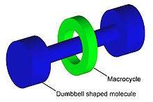
![]()
Graphical representation of a rotaxane, useful as a molecular switch.


![]()
This device transfers energy from nano-thin layers of quantum wells to nanocrystals above them, causing the nanocrystals to emit visible light.[22]
Nanomaterials
The nanomaterials field includes subfields which develop or study materials having unique properties arising from their nanoscale dimensions.[23]
- Interface and colloid science has given rise to many materials which may be useful in nanotechnology, such as carbon nanotubes and other fullerenes, and various nanoparticles and nanorods. Nanomaterials with fast ion transport are related also to nanoionics and nanoelectronics.
- Nanoscale materials can also be used for bulk applications; most present commercial applications of nanotechnology are of this flavor.
- Progress has been made in using these materials for medical applications; see Nanomedicine.
- Nanoscale materials are sometimes used in solar cells which combats the cost of traditional Silicon solar cells
- Development of applications incorporating semiconductor nanoparticles to be used in the next generation of products, such as display technology, lighting, solar cells and biological imaging; see quantum dots.
Bottom-up approaches
These seek to arrange smaller components into more complex assemblies.
- DNA nanotechnology utilizes the specificity of Watson–Crick basepairing to construct well-defined structures out of DNA and other nucleic acids.
- Approaches from the field of «classical» chemical synthesis (inorganic and organic synthesis) also aim at designing molecules with well-defined shape (e.g. bis-peptides[24]).
- More generally, molecular self-assembly seeks to use concepts of supramolecular chemistry, and molecular recognition in particular, to cause single-molecule components to automatically arrange themselves into some useful conformation.
- Atomic force microscope tips can be used as a nanoscale «write head» to deposit a chemical upon a surface in a desired pattern in a process called dip pen nanolithography. This technique fits into the larger subfield of nanolithography.
Top-down approaches
These seek to create smaller devices by using larger ones to direct their assembly.
- Many technologies that descended from conventional solid-state silicon methods for fabricating microprocessors are now capable of creating features smaller than 100 nm, falling under the definition of nanotechnology. Giant magnetoresistance-based hard drives already on the market fit this description,[25] as do atomic layer deposition (ALD) techniques. Peter Grünberg and Albert Fert received the Nobel Prize in Physics in 2007 for their discovery of Giant magnetoresistance and contributions to the field of spintronics.[26]
- Solid-state techniques can also be used to create devices known as nanoelectromechanical systems or NEMS, which are related to microelectromechanical systems or MEMS.
- Focused ion beams can directly remove material, or even deposit material when suitable pre-cursor gasses are applied at the same time. For example, this technique is used routinely to create sub-100 nm sections of material for analysis in Transmission electron microscopy.
- Atomic force microscope tips can be used as a nanoscale «write head» to deposit a resist, which is then followed by an etching process to remove material in a top-down method.
Functional approaches
These seek to develop components of a desired functionality without regard to how they might be assembled.
- Molecular scale electronics seeks to develop molecules with useful electronic properties. These could then be used as single-molecule components in a nanoelectronic device.[27] For an example see rotaxane.
- Synthetic chemical methods can also be used to create synthetic molecular motors, such as in a so-called nanocar.
Biomimetic approaches
- Bionics or biomimicry seeks to apply biological methods and systems found in nature, to the study and design of engineering systems and modern technology. Biomineralization is one example of the systems studied.
- Bionanotechnology is the use of biomolecules for applications in nanotechnology, including use of viruses.[28] Nanocellulose is a potential bulk-scale application.
Speculative
These subfields seek to anticipate what inventions nanotechnology might yield, or attempt to propose an agenda along which inquiry might progress. These often take a big-picture view of nanotechnology, with more emphasis on its societal implications than the details of how such inventions could actually be created.
- Molecular nanotechnology is a proposed approach which involves manipulating single molecules in finely controlled, deterministic ways. This is more theoretical than the other subfields and is beyond current capabilities.
- Nanorobotics centers on self-sufficient machines of some functionality operating at the nanoscale. There are hopes for applying nanorobots in medicine,[29][30][31] but it may not be easy to do such a thing because of several drawbacks of such devices.[32] Nevertheless, progress on innovative materials and methodologies has been demonstrated with some patents granted about new nanomanufacturing devices for future commercial applications, which also progressively helps in the development towards nanorobots with the use of embedded nanobioelectronics concepts.[33][34]
- Productive nanosystems are «systems of nanosystems» which will be complex nanosystems that produce atomically precise parts for other nanosystems, not necessarily using novel nanoscale-emergent properties, but well-understood fundamentals of manufacturing. Because of the discrete (i.e. atomic) nature of matter and the possibility of exponential growth, this stage is seen as the basis of another industrial revolution. Mihail Roco, one of the architects of the USA’s National Nanotechnology Initiative, has proposed four states of nanotechnology that seem to parallel the technical progress of the Industrial Revolution, progressing from passive nanostructures to active nanodevices to complex nanomachines and ultimately to productive nanosystems.[35]
- Programmable matter seeks to design materials whose properties can be easily, reversibly and externally controlled though a fusion of information science and materials science.
- Due to the popularity and media exposure of the term nanotechnology, the words picotechnology and femtotechnology have been coined in analogy to it, although these are only used rarely and informally.
Tools and techniques
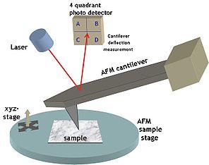
![]()
Typical AFM setup. A microfabricated cantilever with a sharp tip is deflected by features on a sample surface, much like in a phonograph but on a much smaller scale. A laser beam reflects off the backside of the cantilever into a set of photodetectors, allowing the deflection to be measured and assembled into an image of the surface.
There are several important modern developments. The atomic force microscope (AFM) and the Scanning Tunneling Microscope (STM) are two early versions of scanning probes that launched nanotechnology. There are other types of scanning probe microscopy, all flowing from the ideas of the scanning confocal microscope developed by Marvin Minsky in 1961 and the scanning acoustic microscope (SAM) developed by Calvin Quate and coworkers in the 1970s, that made it possible to see structures at the nanoscale. The tip of a scanning probe can also be used to manipulate nanostructures (a process called positional assembly). Feature-oriented scanning-positioning methodology suggested by Rostislav Lapshin appears to be a promising way to implement these nanomanipulations in automatic mode.[36] However, this is still a slow process because of low scanning velocity of the microscope. Various techniques of nanolithography such as optical lithography, X-ray lithography dip pen nanolithography, electron beam lithography or nanoimprint lithography were also developed. Lithography is a top-down fabrication technique where a bulk material is reduced in size to nanoscale pattern.
Another group of nanotechnological techniques include those used for fabrication of nanotubes and nanowires, those used in semiconductor fabrication such as deep ultraviolet lithography, electron beam lithography, focused ion beam machining, nanoimprint lithography, atomic layer deposition, and molecular vapor deposition, and further including molecular self-assembly techniques such as those employing di-block copolymers. However, all of these techniques preceded the nanotech era, and are extensions in the development of scientific advancements rather than techniques which were devised with the sole purpose of creating nanotechnology and which were results of nanotechnology research.
The top-down approach anticipates nanodevices that must be built piece by piece in stages, much as manufactured items are made. Scanning probe microscopy is an important technique both for characterization and synthesis of nanomaterials. Atomic force microscopes and scanning tunneling microscopes can be used to look at surfaces and to move atoms around. By designing different tips for these microscopes, they can be used for carving out structures on surfaces and to help guide self-assembling structures. By using, for example, feature-oriented scanning-positioning approach, atoms can be moved around on a surface with scanning probe microscopy techniques.[36] At present, it is expensive and time-consuming for mass production but very suitable for laboratory experimentation.
In contrast, bottom-up techniques build or grow larger structures atom by atom or molecule by molecule. These techniques include chemical synthesis, self-assembly and positional assembly. Dual polarisation interferometry is one tool suitable for characterisation of self assembled thin films. Another variation of the bottom-up approach is molecular beam epitaxy or MBE. Researchers at Bell Telephone Laboratories like John R. Arthur. Alfred Y. Cho, and Art C. Gossard developed and implemented MBE as a research tool in the late 1960s and 1970s. Samples made by MBE were key to the discovery of the fractional quantum Hall effect for which the 1998 Nobel Prize in Physics was awarded. MBE allows scientists to lay down atomically precise layers of atoms and, in the process, build up complex structures. Important for research on semiconductors, MBE is also widely used to make samples and devices for the newly emerging field of spintronics.
However, new therapeutic products, based on responsive nanomaterials, such as the ultradeformable, stress-sensitive Transfersome vesicles, are under development and already approved for human use in some countries.[citation needed]
Applications
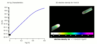
![]()
One of the major applications of nanotechnology is in the area of nanoelectronics with MOSFET’s being made of small nanowires ~10 nm in length. Here is a simulation of such a nanowire.
As of August 21, 2008, the Project on Emerging Nanotechnologies estimates that over 800 manufacturer-identified nanotech products are publicly available, with new ones hitting the market at a pace of 3–4 per week.[9] The project lists all of the products in a publicly accessible online database. Most applications are limited to the use of «first generation» passive nanomaterials which includes titanium dioxide in sunscreen, cosmetics, surface coatings,[37] and some food products; Carbon allotropes used to produce gecko tape; silver in food packaging, clothing, disinfectants and household appliances; zinc oxide in sunscreens and cosmetics, surface coatings, paints and outdoor furniture varnishes; and cerium oxide as a fuel catalyst.[8]
The National Science Foundation (a major distributor for nanotechnology research in the United States) funded researcher David Berube to study the field of nanotechnology. His findings are published in the monograph Nano-Hype: The Truth Behind the Nanotechnology Buzz. This study concludes that much of what is sold as “nanotechnology” is in fact a recasting of straightforward materials science, which is leading to a “nanotech industry built solely on selling nanotubes, nanowires, and the like” which will “end up with a few suppliers selling low margin products in huge volumes.» Further applications which require actual manipulation or arrangement of nanoscale components await further research. Though technologies branded with the term ‘nano’ are sometimes little related to and fall far short of the most ambitious and transformative technological goals of the sort in molecular manufacturing proposals, the term still connotes such ideas. According to Berube, there may be a danger that a «nano bubble» will form, or is forming already, from the use of the term by scientists and entrepreneurs to garner funding, regardless of interest in the transformative possibilities of more ambitious and far-sighted work.[38]
Nanoproducts
Nanoproducts are considered to be consumer goods that have been enhanced by nanotechnology in some form.
The consumer world is seeing more products being released that have been enhanced with nanotechnology. Experts claim that the most immediate impact of nanotechnology is with everyday consumer products. There are numerous amount of products that have been enhanced with nanotechnology. Tennis balls last longer, golf balls fly straighter, even bowling balls become more endurable and have a harder surface to them. Trousers and socks have been infused with nanotechnology so that they will last longer and keep people cool in the summer. Arcade-size video games of yesteryear have been replaced with games like Madden NFL 2005, Grand Theft Auto, and Halo 2 for the PlayStation, Xbox, and Nintendo Game Cube thanks to nanotechnology.
Without nanotechnology, BlackBerries would not be possible along with flash drives, digital cameras, and even MP3 files. Bandages are being infused with silver nanoparticles to heal cuts faster.[39]
Cars are being manufactured with nanomaterials so they may need fewer metals and less fuel to operate in the future.[40] Video game consoles and personal computers may become cheaper, faster, and contain more memory thanks to nanotechnology.[41] Nanotechnology may have the ability to make existing medical applications cheaper and easier to use in places like the general practitioner’s office and at home.[42]
Implications
Because of the far-ranging claims that have been made about potential applications of nanotechnology, a number of serious concerns have been raised about what effects these will have on our society if realized, and what action if any is appropriate to mitigate these risks.
There are possible dangers that arise with the development of nanotechnology. The Center for Responsible Nanotechnology suggests that new developments could result, among other things, in untraceable weapons of mass destruction, networked cameras for use by the government, and weapons developments fast enough to destabilize arms races («Nanotechnology Basics»).
Public deliberations on risk perception in the US and UK carried out by the Center for Nanotechnology in Society at UCSB found that participants were more positive about nanotechnologies for energy than health applications, with health applications raising moral and ethical dilemmas such as cost and availability.[43]
One area of concern is the effect that industrial-scale manufacturing and use of nanomaterials would have on human health and the environment, as suggested by nanotoxicology research. Groups such as the Center for Responsible Nanotechnology have advocated that nanotechnology should be specially regulated by governments for these reasons. Others counter that overregulation would stifle scientific research and the development of innovations which could greatly benefit mankind.
Other experts, including director of the Woodrow Wilson Center’s Project on Emerging Nanotechnologies David Rejeski, have testified[44] that successful commercialization depends on adequate oversight, risk research strategy, and public engagement. Berkeley, California is currently the only city in the United States to regulate nanotechnology;[45] Cambridge, Massachusetts in 2008 considered enacting a similar law,[46] but ultimately rejected this.[47]
Health and environmental concerns
Some of the recently developed nanoparticle products may have unintended consequences. Researchers have discovered that silver nanoparticles used in socks only to reduce foot odor are being released in the wash with possible negative consequences.[48] Silver nanoparticles, which are bacteriostatic, may then destroy beneficial bacteria which are important for breaking down organic matter in waste treatment plants or farms.[49]
A study at the University of Rochester found that when rats breathed in nanoparticles, the particles settled in the brain and lungs, which led to significant increases in biomarkers for inflammation and stress response.[50] A study in China indicated that nanoparticles induce skin aging through oxidative stress in hairless mice.[51][52]
A two-year study at UCLA’s School of Public Health found lab mice consuming nano-titanium dioxide showed DNA and chromosome damage to a degree «linked to all the big killers of man, namely cancer, heart disease, neurological disease and aging».[53]
A major study published more recently in Nature Nanotechnology suggests some forms of carbon nanotubes – a poster child for the “nanotechnology revolution” – could be as harmful as asbestos if inhaled in sufficient quantities. Anthony Seaton of the Institute of Occupational Medicine in Edinburgh, Scotland, who contributed to the article on carbon nanotubes said «We know that some of them probably have the potential to cause mesothelioma. So those sorts of materials need to be handled very carefully.»[54] In the absence of specific nano-regulation forthcoming from governments, Paull and Lyons (2008) have called for an exclusion of engineered nanoparticles from organic food.[55] A newspaper article reports that workers in a paint factory developed serious lung disease and nanoparticles were found in their lungs.[56]
Regulation
Calls for tighter regulation of nanotechnology have occurred alongside a growing debate related to the human health and safety risks associated with nanotechnology.[57] Furthermore, there is significant debate about who is responsible for the regulation of nanotechnology. While some non-nanotechnology specific regulatory agencies currently cover some products and processes (to varying degrees) – by “bolting on” nanotechnology to existing regulations – there are clear gaps in these regimes.[58] In «Nanotechnology Oversight: An Agenda for the Next Administration,»[59] former EPA deputy administrator J. Clarence (Terry) Davies lays out a clear regulatory roadmap for the next presidential administration and describes the immediate and longer term steps necessary to deal with the current shortcomings of nanotechnology oversight.
Stakeholders concerned by the lack of a regulatory framework to assess and control risks associated with the release of nanoparticles and nanotubes have drawn parallels with bovine spongiform encephalopathy (‘mad cow’s disease), thalidomide, genetically modified food,[60] nuclear energy, reproductive technologies, biotechnology, and asbestosis. Dr. Andrew Maynard, chief science advisor to the Woodrow Wilson Center’s Project on Emerging Nanotechnologies, concludes (among others) that there is insufficient funding for human health and safety research, and as a result there is currently limited understanding of the human health and safety risks associated with nanotechnology.[61] As a result, some academics have called for stricter application of the precautionary principle, with delayed marketing approval, enhanced labelling and additional safety data development requirements in relation to certain forms of nanotechnology.[62]
The Royal Society report[6] identified a risk of nanoparticles or nanotubes being released during disposal, destruction and recycling, and recommended that “manufacturers of products that fall under extended producer responsibility regimes such as end-of-life regulations publish procedures outlining how these materials will be managed to minimize possible human and environmental exposure” (p.xiii). Reflecting the challenges for ensuring responsible life cycle regulation, the Institute for Food and Agricultural Standards has proposed standards for nanotechnology research and development should be integrated across consumer, worker and environmental standards. They also propose that NGOs and other citizen groups play a meaningful role in the development of these standards.
The Center for Nanotechnology in Society at UCSB has found that people respond differently to nanotechnologies based upon application — with participants in public deliberations more positive about nanotechnologies for energy than health applications — suggesting that any public calls for nano regulations may differ by technology sector.[43]
See also
- Bionanoscience
- Energy applications of nanotechnology
- List of emerging technologies
- List of software for nanostructures modeling
- Materiomics
- Molecular design software
- Molecular mechanics
- Nanoengineering
- Nanobiotechnology
- Nanofluidics
- Nanohub
- Nanometrology
- Nanoscale networks
- Nanotechnology education
- Nanotechnology in water treatment
- Nanothermite
- Nanoweapons
- Top-down and bottom-up
- Translational research
- Wet nanotechnology
References
- ^ Cristina Buzea, Ivan Pacheco, and Kevin Robbie (2007). «Nanomaterials and Nanoparticles: Sources and Toxicity». Biointerphases 2: MR17. doi:10.1116/1.2815690. PMID 20419892.
- ^ Binnig, G.; Rohrer, H. (1986). «Scanning tunneling microscopy». IBM Journal of Research and Development 30: 4.
- ^ «Press Release: the 1996 Nobel Prize in Physics». Nobelprize.org. 15 October 1986. http://nobelprize.org/nobel_prizes/physics/laureates/1986/press.html. Retrieved 12 May 2011.
- ^ Kroto, H. W.; Heath, J. R.; O’Brien, S. C.; Curl, R. F.; Smalley, R. E. (1985). «C60: Buckminsterfullerene». Nature 318 (6042): 162–163. Bibcode 1985Natur.318..162K. doi:10.1038/318162a0.
- ^ Adams, W Wade; Baughman, Ray H (2005). «Retrospective: Richard E. Smalley (1943-2005)». Science 310 (5756): pp. 1916. 2005 Dec 23. doi:10.1126/science.1122120. PMID 16373566
- ^ a b «Nanoscience and nanotechnologies: opportunities and uncertainties». Royal Society and Royal Academy of Engineering. July 2004. http://www.nanotec.org.uk/finalReport.htm. Retrieved 13 May 2011.
- ^ «Nanotechnology: Drexler and Smalley make the case for and against ‘molecular assemblers'». Chemical & Engineering News (American Chemical Society) 81 (48): 37–42. 1 December 2003. http://pubs.acs.org/cen/coverstory/8148/8148counterpoint.html. Retrieved 9 May 2010.
- ^ a b «Nanotechnology Information Center: Properties, Applications, Research, and Safety Guidelines». American Elements. http://www.americanelements.com/nanotech.htm. Retrieved 13 May 2011.
- ^ a b «Analysis: This is the first publicly available on-line inventory of nanotechnology-based consumer products». The Project on Emerging Nanotechnologies. 2008. http://www.nanotechproject.org/inventories/consumer/analysis_draft/. Retrieved 13 May 2011.
- ^ Fritz Allhoff, Patrick Lin, Daniel Moore, What is nanotechnology and why does it matter?: from science to ethics, pp.3-5, John Wiley and Sons, 2010 ISBN 1405175451.
- ^ S.K. Prasad, Modern Concepts in Nanotechnology, pp.31-32, Discovery Publishing House, 2008 ISBN 8183562965.
- ^ a b Kahn, Jennifer (2006). «Nanotechnology». National Geographic 2006 (June): 98–119.
- ^ Rodgers, P. (2006). «Nanoelectronics: Single file». Nature Nanotechnology. doi:10.1038/nnano.2006.5.
- ^ Lubick N (2008). «Silver socks have cloudy lining». Environ Sci Technol 42 (11): 3910. PMID 18589943.
- ^ Nanotechnology: Developing Molecular Manufacturing
- ^ «Some papers by K. Eric Drexler». http://www.imm.org/PNAS.html.
- ^ California NanoSystems Institute
- ^ C&En: Cover Story — Nanotechnology
- ^ Regan, BC; Aloni, S; Jensen, K; Ritchie, RO; Zettl, A (2005). «Nanocrystal-powered nanomotor». Nano letters 5 (9): 1730–3. Bibcode 2005NanoL…5.1730R. doi:10.1021/nl0510659. PMID 16159214. http://www.physics.berkeley.edu/research/zettl/pdf/312.NanoLett5regan.pdf.
- ^ Regan, B. C.; Aloni, S.; Jensen, K.; Zettl, A. (2005). «Surface-tension-driven nanoelectromechanical relaxation oscillator». Applied Physics Letters 86 (12): 123119. Bibcode 2005ApPhL..86l3119R. doi:10.1063/1.1887827. http://www.lbl.gov/Science-Articles/Archive/sabl/2005/May/Tiniest-Motor.pdf.
- ^ Goodman, R.P.; Schaap, I.A.T.; Tardin, C.F.; Erben, C.M.; Berry, R.M.; Schmidt, C.F.; Turberfield, A.J. (9 December 2005). «Rapid chiral assembly of rigid DNA building blocks for molecular nanofabrication». Science 310 (5754): 1661–1665. Bibcode 2005Sci…310.1661G. doi:10.1126/science.1120367. ISSN 0036-8075. PMID 16339440.
- ^ Wireless nanocrystals efficiently radiate visible light
- ^ Clarkson, AJ; Buckingham, DA; Rogers, AJ; Blackman, AG; Clark, CR (2004). «Nanostructured Ceramics in Medical Devices: Applications and Prospects». JOM 56 (10): 38–43. Bibcode 2004JOM….56j..38N. doi:10.1007/s11837-004-0289-x. PMID 11196953.
- ^ Levins, Christopher G.; Schafmeister, Christian E. (2006). «The Synthesis of Curved and Linear Structures from a Minimal Set of Monomers». ChemInform 37 (5). doi:10.1002/chin.200605222.
- ^ «Applications/Products». National Nanotechnology Initiative. http://www.nano.gov/html/facts/appsprod.html. Retrieved 2007-10-19.
- ^ «The Nobel Prize in Physics 2007». Nobelprize.org. http://nobelprize.org/nobel_prizes/physics/laureates/2007/index.html. Retrieved 2007-10-19.
- ^ Das S, Gates AJ, Abdu HA, Rose GS, Picconatto CA, Ellenbogen JC. (2007). «Designs for Ultra-Tiny, Special-Purpose Nanoelectronic Circuits». IEEE Transactions on Circuits and Systems I 54 (11): 2528–2540. doi:10.1109/TCSI.2007.907864.
- ^ C.Michael Hogan. 2010. Virus. Encyclopedia of Earth. National Council for Science and the Environment. eds. S.Draggan and C.Cleveland
- ^ Ghalanbor Z, Marashi SA, Ranjbar B (2005). «Nanotechnology helps medicine: nanoscale swimmers and their future applications». Med Hypotheses 65 (1): 198–199. doi:10.1016/j.mehy.2005.01.023. PMID 15893147.
- ^ Kubik T, Bogunia-Kubik K, Sugisaka M. (2005). «Nanotechnology on duty in medical applications». Curr Pharm Biotechnol. 6 (1): 17–33. PMID 15727553.
- ^ Leary, SP; Liu, CY; Apuzzo, ML (2006). «Toward the Emergence of Nanoneurosurgery: Part III-Nanomedicine: Targeted Nanotherapy, Nanosurgery, and Progress Toward the Realization of Nanoneurosurgery». Neurosurgery 58 (6): 1009–1026. doi:10.1227/01.NEU.0000217016.79256.16. PMID 16723880.
- ^ Shetty RC (2005). «Potential pitfalls of nanotechnology in its applications to medicine: immune incompatibility of nanodevices». Med Hypotheses 65 (5): 998–9. doi:10.1016/j.mehy.2005.05.022. PMID 16023299.
- ^ Cavalcanti A, Shirinzadeh B, Freitas RA Jr., Kretly LC. (2007). «Medical Nanorobot Architecture Based on Nanobioelectronics». Recent Patents on Nanotechnology. 1 (1): 1–10. doi:10.2174/187221007779814745.
- ^ Boukallel M, Gauthier M, Dauge M, Piat E, Abadie J. (2007). «Smart microrobots for mechanical cell characterization and cell convoying». IEEE Trans. Biomed. Eng. 54 (8): 1536–40. doi:10.1109/TBME.2007.891171. PMID 17694877.
- ^ «International Perspective on Government Nanotechnology Funding in 2005». http://www.nsf.gov/crssprgm/nano/reports/mcr_05-0526_intpersp_nano.pdf.
- ^ a b R. V. Lapshin (2004). «Feature-oriented scanning methodology for probe microscopy and nanotechnology» (PDF). Nanotechnology (UK: IOP) 15 (9): 1135–1151. Bibcode 2004Nanot..15.1135L. doi:10.1088/0957-4484/15/9/006. ISSN 0957-4484. http://www.nanoworld.org/homepages/lapshin/publications.htm#feature2004.
- ^ Kurtoglu M. E., Longenbach T., Reddington P., Gogotsi Y. (2011). «Effect of Calcination Temperature and Environment on Photocatalytic and Mechanical Properties of Ultrathin Sol–Gel Titanium Dioxide Films». Journal of the American Ceramic Society 94: 1101–1108. doi:10.1111/j.1551-2916.2010.04218.x.
- ^ Berube, David (2006). Nano-Hype: The Truth Behind the Nanotechnology Buzz. Amherst, NY: Prometheus Books. http://www.prometheusbooks.com/index.php?main_page=product_info&products_id=1822/.
- ^ Real World Applications of Nanotechnology at NNIN.org
- ^ Nano in transport at NanoandMe.org
- ^ Nano in computing and electronics at NanoandMe.org
- ^ Nano in medicine at NanoandMe.org
- ^ a b Barbara Herr Harthorn, «People in the US and the UK show strong similarities in their attitudes toward nanotechnologies» Nanotechnology Today, January 23, 2009.
- ^ Testimony of David Rejeski for U.S. Senate Committee on Commerce, Science and Transportation Project on Emerging Nanotechnologies. Retrieved on 2008-3-7.
- ^ Berkeley considering need for nano safety (Rick DelVecchio, Chronicle Staff Writer) Friday, November 24, 2006
- ^ Cambridge considers nanotech curbs — City may mimic Berkeley bylaws (By Hiawatha Bray, Boston Globe Staff) January 26, 2007
- ^ Recommendations for a Municipal Health & Safety Policy for Nanomaterials: A Report to the Cambridge City Manager. July 2008.
- ^ Lubick, N. (2008). Silver socks have cloudy lining.
- ^ Murray R.G.E., Advances in Bacterial Paracrystalline Surface Layers (Eds.: T. J. Beveridge, S. F. Koval). Plenum pp. 3 ± 9. [9]
- ^ Elder, A. (2006). Tiny Inhaled Particles Take Easy Route from Nose to Brain.
- ^ Wu, J; Liu, W; Xue, C; Zhou, S; Lan, F; Bi, L; Xu, H; Yang, X et al. (2009). «Toxicity and penetration of TiO2 nanoparticles in hairless mice and porcine skin after subchronic dermal exposure». Toxicology letters 191 (1): 1–8. doi:10.1016/j.toxlet.2009.05.020. PMID 19501137.
- ^ Jonaitis, TS; Card, JW; Magnuson, B (2010). «Concerns regarding nano-sized titanium dioxide dermal penetration and toxicity study». Toxicology letters 192 (2): 268–9. doi:10.1016/j.toxlet.2009.10.007. PMID 19836437.
- ^ Schneider, Andrew, «Amid Nanotech’s Dazzling Promise, Health Risks Grow», March 24, 2010.
- ^ Weiss, R. (2008). Effects of Nanotubes May Lead to Cancer, Study Says.
- ^ Paull, J. & Lyons, K. (2008). «Nanotechnology: The Next Challenge for Organics». Journal of Organic Systems 3: 3–22. http://orgprints.org/13569/1/13569.pdf.
- ^ Smith, Rebecca (August 19, 2009). «Nanoparticles used in paint could kill, research suggests». London: Telegraph. http://www.telegraph.co.uk/health/healthnews/6016639/Nanoparticles-used-in-paint-could-kill-research-suggests.html. Retrieved May 19, 2010.
- ^ Kevin Rollins (Nems Mems Works, LLC). «Nanobiotechnology Regulation: A Proposal for Self-Regulation with Limited Oversight». Volume 6 — Issue 2. http://www.nanolabweb.com/index.cfm/action/main.default.viewArticle/articleID/290/CFID/3564274/CFTOKEN/43473772/index.html. Retrieved 2 September 2010.
- ^ Bowman D, and Hodge G (2006). «Nanotechnology: Mapping the Wild Regulatory Frontier». Futures 38 (9): 1060–1073. doi:10.1016/j.futures.2006.02.017.
- ^ Davies, JC. (2008). Nanotechnology Oversight: An Agenda for the Next Administration.
- ^ Rowe G, Horlick-Jones T, Walls J, Pidgeon N, (2005). «Difficulties in evaluating public engagement initiatives: reflections on an evaluation of the UK GM Nation?». Public Understanding of Science. 14: 333.
- ^ Maynard, A.Testimony by Dr. Andrew Maynard for the U.S. House Committee on Science and Technology. (2008-4-16). Retrieved on 2008-11-24.
- ^ Faunce TA et al. Sunscreen Safety: The Precautionary Principle, The Australian Therapeutic Goods Administration and Nanoparticles in Sunscreens Nanoethics (2008) 2:231–240 DOI 10.1007/s11569-008-0041-z. Thomas Faunce & Katherine Murray & Hitoshi Nasu & Diana Bowman (published online: 24 July 2008). «Sunscreen Safety: The Precautionary Principle, The Australian Therapeutic Goods Administration and Nanoparticles in Sunscreens». Springer Science + Business Media B.V. http://law.anu.edu.au/StaffUploads/236-Nanoethics%20Sunscreens%202008.pdf. Retrieved 18 June 2009.
Further reading
- «Basic Concepts of Nanotechnology» History of Nano-Technology, News, Materials, Potential Risks and Important People.
- «About Nanotechnology — An Introduction to Nanotech from The Project on Emerging Nanotechnologies». Nanotechproject.org. http://www.nanotechproject.org/topics/nano101/. Retrieved 2009-11-24.
- «Nanotechnology Introduction Pages». Nanotech-now.com. http://www.nanotech-now.com/nano_intro.htm. Retrieved 2009-11-24.
- Medicalnanotec.com, Introduction to applications of Nanotechnology in Medicine.
- Maynard, Andrew, «The Twinkie Guide to Nanotechnology • News Archive • Nanotechnology Project». Nanotechproject.org. 2007-10-22. http://www.nanotechproject.org/news/archive/the_twinkie_guide_to_nanotechnology/. Retrieved 2009-11-24. Woodrow Wilson International Center for Scholars. 2007. — «..a friendly, funny, 25-minute travel guide to the technology»
- «Nanotechnology Basics: For Students and Other Learners». Center for Responsible Nanotechnology — World Care. 11 November 2008.
- Fritz Allhoff and Patrick Lin (eds.), Nanotechnology & Society: Current and Emerging Ethical Issues (Dordrecht: Springer, 2008).
- Fritz Allhoff, Patrick Lin, James Moor, and John Weckert (eds.) «Nanoethics: The Ethical and Societal Implications of Nanotechnology». Hoboken: John Wiley & Sons. 2007. http://www.wiley.com/WileyCDA/WileyTitle/productCd-0470084170.html. «Wiley». http://www.nanoethics.org/wiley.html.
- J. Clarence Davies, EPA and Nanotechnology: Oversight for the 21st Century, Project on Emerging Nanotechnologies, PEN 9, May 2007.
- Carl Marziali, «Little Big Science,» USC Trojan Family Magazine, Winter 2007.
- William Sims Bainbridge: Nanoconvergence: The Unity of Nanoscience, Biotechnology, Information Technology and Cognitive Science, June 27, 2007, Prentice Hall, ISBN 0-13-244643-X
- Lynn E. Foster: Nanotechnology: Science, Innovation, and Opportunity, December 21, 2005, Prentice Hall, ISBN 0-13-192756-6
- Impact of Nanotechnology on Biomedical Sciences: Review of Current Concepts on Convergence of Nanotechnology With Biology by Herbert Ernest and Rahul Shetty, from AZojono, May 2005.
- Hunt, G & Mehta, M (eds)(2008) Nanotechnology: Risk, Ethics & Law, Earthscan, London.
- Andrew Schneider, The Nanotech Gamble, Growing Health Risks from Nanomaterials in Food and Medicine, First in a Three-Part Series, AOL News Special Report, March 24, 2010.
- Hari Singh Nalwa (2004), Encyclopedia of Nanoscience and Nanotechnology (10-Volume Set), American Scientific Publishers. ISBN 1-58883-001-2
- Michael Rieth and Wolfram Schommers (2006), Handbook of Theoretical and Computational Nanotechnology (10-Volume Set), American Scientific Publishers. ISBN 1-58883-042-X
- Akhlesh Lakhtakia (ed) (2004). The Handbook of Nanotechnology. Nanometer Structures: Theory, Modeling, and Simulation. SPIE Press, Bellingham, WA, USA. ISBN 0-8194-5186-X.
- Fei Wang & Akhlesh Lakhtakia (eds) (2006). Selected Papers on Nanotechnology—Theory & Modeling (Milestone Volume 182). SPIE Press, Bellingham, WA, USA. ISBN 0-8194-6354-X.
- Jumana Boussey, Georges Kamarinos, Laurent Montès (editors) (2003), Towards Nanotechnology, «Nano et Micro Technologies», Hermes Sciences Publ., Paris, ISBN 2-7462-0858-X.
- The Silicon Valley Toxics Coalition (April, 2008), Regulating Emerging Technologies in Silicon Valley and Beyond
- Genetic Engineering & Biotechnology News (January, 2008), Getting a Handle on Nanobiotech Products Regulators and Companies Are Laying the Groundwork for a Predicted Bright Future
- Suh WH, Suslick KS, Stucky GD, Suh YH (2009). «Nanotechnology, nanotoxicology, and neuroscience». Progress in Neurobiology 87 (3): 133–70. doi:10.1016/j.pneurobio.2008.09.009. PMC 2728462. PMID 18926873. http://www.pubmedcentral.nih.gov/articlerender.fcgi?tool=pmcentrez&artid=2728462.
- RJ Aitken, SM Hankin, B Ross, CL Tran, V Stone, TF Fernandes, K Donaldson, R Duffin, Q Chaudhry, TA Wilkins, SA Wilkins, LS Levy, SA Rocks, A Maynard, EMERGNANO Report, Institute of Occupational Medicine, Report TM/09/01 March 2009.
External links
- Nanotechnology at the Open Directory Project
- What is Nanotechnology? (A Vega/BBC/OU Video Discussion).
- Course on Introduction to Nanotechnology
- Nanex Project
- SAFENANO A nanotechnology initiative of the Institute of Occupational Medicine
| v · d · eNanotechnology (portal) | |
|---|---|
| Overview |
History · Impact · Applications · Regulation · Organizations · Popular culture |
| Nanomaterials |
Fullerene · Carbon nanotubes · Nanoparticles |
| Nanomedicine |
Nanotoxicology · Nanosensor · Nanobiotechnology |
| Molecular self-assembly |
Self-assembled monolayer · Supramolecular assembly · DNA nanotechnology |
| Nanoelectronics |
Molecular electronics · Nanolithography |
| Scanning probe microscopy |
Atomic force microscope · Scanning tunneling microscope |
| Molecular nanotechnology |
Molecular assembler · Nanorobotics · Mechanosynthesis · Nanofoundry · Nanoreactor |
| v · d · eTechnology | |
|---|---|
|
|
| Applied science |
|
| Biomedical |
|
| Domestic |
|
| Educational |
|
| Engineering |
|
| Environmental |
|
| Industry |
|
| Information |
|
| Military |
|
| Transport |
|
| Theories |
|
| Other |
|
|
|
| v · d · eEmerging technologies | ||||||||||||||||||||||||||||||
|---|---|---|---|---|---|---|---|---|---|---|---|---|---|---|---|---|---|---|---|---|---|---|---|---|---|---|---|---|---|---|
|
List of emerging technologies · Technology |
||||||||||||||||||||||||||||||
| Fields |
|
|||||||||||||||||||||||||||||
| Other |
Exploratory engineering · Technology forecasting (Accelerating change · Moore’s law · Timeline of the future in forecasts · Technological singularity) · Transhumanism · Virtusphere |
|||||||||||||||||||||||||||||
|
|
| v · d · eLevels of technological manipulation of matter | |
|---|---|
|
Technology · Orders of magnitude (length) |
|
| Megascale engineering |
Megastructure · Terraforming · Planetary engineering · Astroengineering · Space elevator · Orbital elevator · Kardashev scale · Great Wall of China · Geoengineering |
| Macro-engineering |
Panama Canal · Suez Canal · Atlantropa · Bering Strait bridge · Red Sea dam · Delta Works |
| Microtechnology |
Microelectromechanical systems · micromachinery · Photolithography |
| Nanotechnology |
Molecular nanotechnology · Implications · Regulation · DNA nanotechnology · Molecular scale electronics · Nanomaterials · Wet nanotechnology · Nanobiotechnology · Nanofoundry · Nanoreactor |
| Picotechnology |
Exotic atom · Rydberg atom · Synthetic element · particle accelerator |
| Femtotechnology |
Nucleon · hafnium bomb · Mode-locking · Limits to computation · Pushing Ice · Femtochemistry · Nuclear isomer |
|
History of technology · Timelines of technology · Engineering |
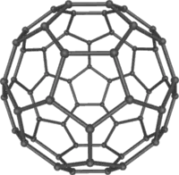
Buckminsterfullerene C60, also known as the buckyball, is the simplest of the carbon structures known as fullerenes. Members of the fullerene family are a major subject of research falling under the nanotechnology umbrella.
Nanotechnology is a field of applied science and technology covering a broad range of topics. The main unifying theme is the control of matter on a scale smaller than 1 micrometer, normally between 1-100 nanometers, as well as the fabrication of devices on this same length scale. It is a highly multidisciplinary field, drawing from fields such as colloidal science, device physics, and supramolecular chemistry. Much speculation exists as to what new science and technology might result from these lines of research. Some view nanotechnology as a marketing term that describes pre-existing lines of research applied to the sub-micron size scale.
Despite the apparent simplicity of this definition, nanotechnology actually encompasses diverse lines of inquiry. Nanotechnology cuts across many disciplines, including colloidal science, chemistry, applied physics, materials science, and even mechanical and electrical engineering. It could variously be seen as an extension of existing sciences into the nanoscale, or as a recasting of existing sciences using a newer, more modern term. Two main approaches are used in nanotechnology: one is a «bottom-up» approach where materials and devices are built from molecular components which assemble themselves chemically using principles of molecular recognition; the other being a «top-down» approach where nano-objects are constructed from larger entities without atomic-level control.
The impetus for nanotechnology has stemmed from a renewed interest in colloidal science, coupled with a new generation of analytical tools such as the atomic force microscope (AFM), and the scanning tunneling microscope (STM). Combined with refined processes such as electron beam lithography and molecular beam epitaxy, these instruments allow the deliberate manipulation of nanostructures, and in turn led to the observation of novel phenomena. The manufacture of polymers based on molecular structure, or the design of computer chip layouts based on surface science are examples of nanotechnology in modern use. Despite the great promise of numerous nanotechnologies such as quantum dots and nanotubes, real applications that have moved out of the lab and into the marketplace have mainly utilized the advantages of colloidal nanoparticles in bulk form, such as suntan lotion, cosmetics, protective coatings, and stain resistant clothing.
|
Nanotechnology
|
|
| Topics | |
|---|---|
| History · Implications Applications · Organizations Popular culture · List of topics |
|
| Subfields and related fields | |
| Nanomedicine Molecular self-assembly Molecular electronics Scanning probe microscopy Nanolithography Molecular nanotechnology |
|
| Nanomaterials | |
| Nanomaterials · Fullerene Carbon nanotubes Fullerene chemistry Applications · Popular culture Timeline · Carbon allotropes Nanoparticles · Quantum dots Colloidal gold · Colloidal silver |
|
| Molecular nanotechnology | |
| Molecular assembler Mechanosynthesis Nanorobotics · Grey goo K. Eric Drexler Engines of Creation |
|
|
|
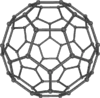
History
Nanoscience and nanotechnology only became possible in the 1910s with the development of the first tools to measure and make nanostructures. But the actual development started with the discovery of electrons and neutrons which showed scientists that matter can really exist on a much smaller scale than what we normally think of as small, and/or what they thought was possible at the time. It was at this time when curiosity for nanostructures had originated.
The atomic force microscope (AFM) and the Scanning Tunneling Microscope (STM) are two early versions of scanning probes that launched nanotechnology. There are other types of scanning probe microscopy, all flowing from the ideas of the scanning confocal microscope developed by Marvin Minsky in 1961 and the scanning acoustic microscope (SAM) developed by Calvin Quate and coworkers in the 1970s, that made it possible to see structures at the nanoscale. The tip of a scanning probe can also be used to manipulate nanostructures (a process called positional assembly). Feature-oriented scanning-positioning methodology suggested by Rostislav Lapshin appears to be a promising way to implement these nanomanipulations in automatic mode. However, this is still a slow process because of low scanning velocity of the microscope. Various techniques of nanolithography such as dip pen nanolithography, electron beam lithography or nanoimprint lithography were also developed. Lithography is a top-down fabrication technique where a bulk material is reduced in size to nanoscale pattern.
The first distinguishing concepts in nanotechnology (but predating use of that name) was in «There’s Plenty of Room at the Bottom,» a talk given by physicist Richard Feynman at an American Physical Society meeting at Caltech on December 29, 1959 [1]. Feynman described a process by which the ability to manipulate individual atoms and molecules might be developed, using one set of precise tools to build and operate another proportionally smaller set, so on down to the needed scale. In the course of this, he noted, scaling issues would arise from the changing magnitude of various physical phenomena: gravity would become less important, surface tension and Van der Waals attraction would become more important. This basic idea appears feasible, and exponential assembly enhances it with parallelism to produce a useful quantity of end products.

Eight allotropes of Carbon
The term «nanotechnology» was defined by Tokyo Science University Professor Norio Taniguchi in a 1974 paper [2] as follows: «‘Nano-technology’ mainly consists of the processing of, separation, consolidation, and deformation of materials by one atom or by one molecule.» In the 1980s the basic idea of this definition was explored in much more depth by Dr. K. Eric Drexler, who promoted the technological significance of nano-scale phenomena and devices through speeches and the book Engines of Creation: The Coming Era of Nanotechnology[3], and so the term acquired its current sense.
Nanotechnology and nanoscience got started in the early 1980s with two major developments; the birth of cluster science and the invention of the scanning tunneling microscope (STM). This development led to the discovery of fullerenes in 1986 and carbon nanotubes a few years later. In another development, the synthesis and properties of semiconductor nanocrystals was studied. This led to a fast increasing number of metal oxide nanoparticles of quantum dots. The atomic force microscope was invented five years after the STM was invented. The AFM uses atomic force to «see» the atoms.
Fundamental concepts
One nanometer (nm) is one billionth, or 10-9 of a meter. For comparison, typical carbon-carbon bond lengths, or the spacing between these atoms in a molecule, are in the range .12-.15 nm, and a DNA double-helix has a diameter around 2 nm. On the other hand, the smallest cellular lifeforms, the bacteria of the genus Mycoplasma, are around 200 nm in length.
Larger to smaller: a materials perspective
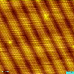
Image of reconstruction on a clean Au(100) surface, as visualized using scanning tunneling microscopy. The individual atoms composing the surface are visible.
A unique aspect of nanotechnology is the vastly increased ratio of surface area to volume present in many nanoscale materials which opens new possibilities in surface-based science, such as catalysis. A number of physical phenomena become noticeably pronounced as the size of the system decreases. These include statistical mechanical effects, as well as quantum mechanical effects, for example the “quantum size effect” where the electronic properties of solids are altered with great reductions in particle size. This effect does not come into play by going from macro to micro dimensions. However, it becomes dominant when the nanometer size range is reached. Additionally, a number of physical properties change when compared to macroscopic systems. One example is the increase in surface area to volume of materials.
Materials reduced to the nanoscale can suddenly show very different properties compared to what they exhibit on a macroscale, enabling unique applications. For instance, opaque substances become transparent (copper); inert materials become catalysts (platinum); stable materials turn combustible (aluminum); solids turn into liquids at room temperature (gold); insulators become conductors (silicon). A material such as gold, which is chemically inert at normal scales, can serve as a potent chemical catalyst at nanoscales. Much of the fascination with nanotechnology stems from these unique quantum and surface phenomena that matter exhibits at the nanoscale.
Simple to complex: a molecular perspective
Modern synthetic chemistry has reached the point where it is possible to prepare small molecules to almost any structure. These methods are used today to produce a wide variety of useful chemicals such as pharmaceuticals or commercial polymers. This ability raises the question of extending this kind of control to the next-larger level, seeking methods to assemble these single molecules into supramolecular assemblies consisting of many molecules arranged in a well defined manner.
These approaches utilize the concepts of molecular self-assembly and/or supramolecular chemistry to automatically arrange themselves into some useful conformation through a bottom-up approach. The concept of molecular recognition is especially important: molecules can be designed so that a specific conformation or arrangement is favored. The Watson-Crick basepairing rules are a direct result of this, as is the specificity of an enzyme being targeted to a single substrate, or the specific folding of the protein itself. Thus, two or more components can be designed to be complementary and mutually attractive so that they make a more complex and useful whole.
Such bottom-up approaches should, broadly speaking, be able to produce devices in parallel and much cheaper than top-down methods, but could potentially be overwhelmed as the size and complexity of the desired assembly increases. Most useful structures require complex and thermodynamically unlikely arrangements of atoms. Nevertheless, there are many examples of self-assembly based on molecular recognition in biology, most notably Watson-Crick basepairing and enzyme-substrate interactions. The challenge for nanotechnology is whether these principles can be used to engineer novel constructs in addition to natural ones.
Molecular nanotechnology
Molecular nanotechnology, sometimes called molecular manufacturing, is a term given to the concept of engineered nanosystems (nanoscale machines) operating on the molecular scale. It is especially associated with the concept of a molecular assembler, a machine that can produce a desired structure or device atom-by-atom using the principles of mechanosynthesis. Manufacturing in the context of productive nanosystems is not related to, and should be clearly distinguished from, the conventional technologies used to manufacture nanomaterials such as carbon nanotubes and nanoparticles.
When the term «nanotechnology» was independently coined and popularized by Eric Drexler (who at the time was unaware of an earlier usage by Norio Taniguchi) it referred to a future manufacturing technology based on molecular machine systems. The premise was that molecular-scale biological analogies of traditional machine components demonstrated molecular machines were possible: by the countless examples found in biology, it is known that billions of years of evolutionary feedback can produce sophisticated, stochastically optimized biological machines. It is hoped that developments in nanotechnology will make possible their construction by some other means, perhaps using biomimetic principles. However, Drexler and other researchers have proposed that advanced nanotechnology, although perhaps initially implemented by biomimetic means, ultimately could be based on mechanical engineering principles, namely, a manufacturing technology based on the mechanical functionality of these components (such as gears, bearings, motors, and structural members) that would enable programmable, positional assembly to atomic specification PNAS-1981. The physics and engineering performance of exemplar designs were analyzed in Drexler’s book [4]. But Drexler’s analysis is very qualitative and does not address very pressing issues, such as the «fat fingers» and «Sticky fingers» problems, which are problems related to the difficulty in handling and assembling on the nanoscale. In general it is very difficult to assemble devices on the atomic scale, as all one has to position atoms are other atoms of comparable size and stickiness.
Another view, put forth by Carlo Montemagno [5] is that future nanosystems will be hybrids of silicon technology and biological molecular machines. Yet another view, put forward by the late Richard Smalley, is that mechanosynthesis is impossible due to the difficulties in mechanically manipulating individual molecules. This led to an exchange of letters [6] in the ACS publication Chemical & Engineering News in 2003.
Though biology clearly demonstrates that molecular machine systems are possible, non-biological molecular machines are today only in their infancy. Leaders in research on non-biological molecular machines are Dr. Alex Zettl and his colleagues at Lawrence Berkeley Laboratories and UC Berkeley. They have constructed at least three distinct molecular devices whose motion is controlled from the desktop with changing voltage: a nanotube nanomotor, a molecular actuator [7], and a nanoelectromechanical relaxation oscillator [8] An experiment indicating that positional molecular assembly is possible was performed by Ho and Lee at Cornell University in 1999. They used a scanning tunneling microscope to move an individual carbon monoxide molecule (CO) to an individual iron atom (Fe) sitting on a flat silver crystal, and chemically bound the CO to the Fe by applying a voltage.
Current research

Graphical representation of a rotaxane, useful as a molecular switch.
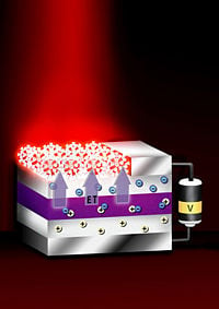
This device transfers energy from nano-thin layers of quantum wells to nanocrystals above them, causing the nanocrystals to emit visible light [9]
Nanotechnology is a very broad term, there are many different but sometimes overlapping subfields that could fall under its umbrella. The following avenues of research could be considered subfields of nanotechnology. Note that these categories are not concrete and a single subfield may overlap many of them, especially as the field of nanotechnology continues to mature.
Nanomaterials
This includes subfields which develop or study materials having unique properties arising from their nanoscale dimensions.
- Colloid science has given rise to many materials which may be useful in nanotechnology, such as carbon nanotubes and other fullerenes, and various nanoparticles and nanorods.
- Nanoscale materials can also be used for bulk applications; most present commercial applications of nanotechnology are of this flavor.
- Progress has been made in using these materials for medical applications.
Bottom-up approaches
These seek to arrange smaller components into more complex assemblies.
- DNA Nanotechnology utilizes the specificity of Watson-Crick basepairing to construct well-defined structures out of DNA and other nucleic acids.
- More generally, molecular self-assembly seeks to use concepts of supramolecular chemistry, and molecular recognition in particular, to cause single-molecule components to automatically arrange themselves into some useful conformation.
Top-down approaches
These seek to create smaller devices by using larger ones to direct their assembly.
- Many technologies descended from conventional solid-state silicon methods for fabricating microprocessors are now capable of creating features smaller than 100 nm, falling under the definition of nanotechnology. Giant magnetoresistance-based hard disk drives already on the market fit this description, as do atomic layer deposition (ALD) techniques.
- Solid-state techniques can also be used to create devices known as nanoelectromechanical systems or NEMS, which are related to microelectromechanical systems (MEMS).
- Atomic force microscope tips can be used as a nanoscale «write head» to deposit a chemical on a surface in a desired pattern in a process called dip pen nanolithography. This fits into the larger subfield of nanolithography.
Functional approaches
These seek to develop components of a desired functionality without regard to how they might be assembled.
- Molecular electronics seeks to develop molecules with useful electronic properties. These could then be used as single-molecule components in a nanoelectronic device.
- Synthetic chemical methods can also be used to create synthetic molecular motors, such as in a so-called nanocar.
Speculative
These subfields seek to anticipate what inventions nanotechnology might yield, or attempt to propose an agenda along which inquiry might progress. These often take a big-picture view of nanotechnology, with more emphasis on its societal implications than the details of how such inventions could actually be created.
- Molecular nanotechnology is a proposed approach which involves manipulating single molecules in finely controlled, deterministic ways. This is more theoretical than the other subfields and is beyond current capabilities.
- Nanorobotics centers on self-sufficient machines of some functionality operating at the nanoscale. There are hopes for applying nanorobots in medicine [10] [11] [12], while it might not be easy to do such a thing because of several drawbacks of such devices
[13] Nevertheless, progress on innovative materials and methodologies has been demonstrated with some patents granted about new nanomanufacturing devices for future commercial applications, which also progressively helps in the development towards nanorobots with the use of embedded nanobioelectronics concept.
- Programmable matter based on artificial atoms seeks to design materials whose properties can be easily and reversibly externally controlled.
- Due to the popularity and media exposure of the term nanotechnology, the words picotechnology and femtotechnology have been coined in analogy to it, although these are only used rarely and informally.
Tools and techniques

Typical AFM setup. A microfabricated cantilever with a sharp tip is deflected by features on a sample surface, much like in a phonograph but on a much smaller scale. A laser beam reflects off the backside of the cantilever into a set of photodetectors, allowing the deflection to be measured and assembled into an image of the surface.
Another technique uses SPT™s (surface patterning tool) as the molecular “ink cartridge.” Each SPT is a microcantilever-based micro-fluidic handling device. SPTs contain either a single microcantilever print head or multiple microcantilevers for simultaneous printing of multiple molecular species. The integrated microfluidic network transports fluid samples from reservoirs located on the SPT through microchannels to the distal end of the cantilever. Thus SPTs can be used to print materials that include biological samples such as proteins, DNA, RNA, and whole viruses, as well as non-biological samples such as chemical solutions, colloids and particle suspensions. SPTs are most commonly used with molecular printers.
Nanotechnological techniques include those used for fabrication of nanowires, those used in semiconductor fabrication such as deep ultraviolet lithography, electron beam lithography, focused ion beam machining, nanoimprint lithography, atomic layer deposition, and molecular vapor deposition, and further including molecular self-assembly techniques such as those employing di-block copolymers. However, all of these techniques preceded the nanotech era, and are extensions in the development of scientific advancements rather than techniques which were devised with the sole purpose of creating nanotechnology and which were results of nanotechnology research.
The top-down approach anticipates nanodevices that must be built piece by piece in stages, much as manufactured items are currently made. Scanning probe microscopy is an important technique both for characterization and synthesis of nanomaterials. Atomic force microscopes and scanning tunneling microscopes can be used to look at surfaces and to move atoms around. By designing different tips for these microscopes, they can be used for carving out structures on surfaces and to help guide self-assembling structures. By using, for example, feature-oriented scanning-positioning approach, atoms can be moved around on a surface with scanning probe microscopy techniques. At present, it is expensive and time-consuming for mass production but very suitable for laboratory experimentation.
In contrast, bottom-up techniques build or grow larger structures atom by atom or molecule by molecule. These techniques include chemical synthesis, self-assembly and positional assembly. Another variation of the bottom-up approach is molecular beam epitaxy or MBE. Researchers at Bell Telephone Laboratories like John R. Arthur, Alfred Y. Cho, and Art C. Gossard developed and implemented MBE as a research tool in the late 1960s and 1970s. Samples made by MBE were key to the discovery of the fractional quantum Hall effect for which the 1998 Nobel Prize in Physics was awarded. MBE allows scientists to lay down atomically-precise layers of atoms and, in the process, build up complex structures. Important for research on semiconductors, MBE is also widely used to make samples and devices for the newly emerging field of spintronics.
Newer techniques such as Dual Polarization Interferometry are enabling scientists to measure quantitatively the molecular interactions that take place at the nano-scale.
Applications
Although there has been much hype about the potential applications of nanotechnology, most current commercialized applications are limited to the use of «first generation» passive nanomaterials. These include titanium dioxide nanoparticles in sunscreen, cosmetics and some food products; silver nanoparticles in food packaging, clothing, disinfectants and household appliances; zinc oxide nanoparticles in sunscreens and cosmetics, surface coatings, paints and outdoor furniture varnishes; and cerium oxide nanoparticles as a fuel catalyst. The Woodrow Wilson Center for International Scholars’ Project on Emerging Nanotechnologies hosts an inventory of consumer products which now contain nanomaterials[14]
However further applications which require actual manipulation or arrangement of nanoscale components await further research. Though technologies currently branded with the term ‘nano’ are sometimes little related to and fall far short of the most ambitious and transformative technological goals of the sort in molecular manufacturing proposals, the term still connotes such ideas. Thus there may be a danger that a «nano bubble» will form, or is forming already, from the use of the term by scientists and entrepreneurs to garner funding, regardless of interest in the transformative possibilities of more ambitious and far-sighted work.
The National Science Foundation (a major source of funding for nanotechnology in the United States) funded researcher David Berube to study the field of nanotechnology. His findings are published in the monograph “Nano-Hype: The Truth Behind the Nanotechnology Buzz.[15]» This published study concludes that much of what is sold as “nanotechnology” is in fact a recasting of straightforward materials science, which is leading to a “nanotech industry built solely on selling nanotubes, nanowires, and the like” which will “end up with a few suppliers selling low margin products in huge volumes.»
Implications
Due to the far-ranging claims that have been made about potential applications of nanotechnology, a number of concerns have been raised about what effects these will have on our society if realized, and what action if any is appropriate to mitigate these risks. Short-term issues include the effects that widespread use of nanomaterials would have on human health and the environment. Longer-term concerns center on the implications that new technologies will have for society at large, and whether these could possibly lead to either a post scarcity economy, or alternatively exacerbate the wealth gap between developed and developing nations.
Health and environmental issues
There is a growing body of scientific evidence which demonstrates the potential for some nanomaterials to be toxic to humans or the environment [16][17][18].
The smaller a particle, the greater its surface area to volume ratio and the higher its chemical reactivity and biological activity. The greater chemical reactivity of nanomaterials results in increased production of reactive oxygen species (ROS), including free radicals. ROS production has been found in a diverse range of nanomaterials including carbon fullerenes, carbon nanotubes and nanoparticle metal oxides. ROS and free radical production is one of the primary mechanisms of nanoparticle toxicity; it may result in oxidative stress, inflammation, and consequent damage to proteins, membranes and DNA [19].
The extremely small size of nanomaterials also means that they are much more readily taken up by the human body than larger sized particles. Nanomaterials are able to cross biological membranes and access cells, tissues and organs that larger-sized particles normally cannot. Nanomaterials can gain access to the blood stream following inhalation or ingestion . At least some nanomaterials can penetrate the skin; even larger microparticles may penetrate skin when it is flexed . Broken skin is an ineffective particle barrier, suggesting that acne, eczema, wounds or severe sunburn may enable skin uptake of nanomaterials more readily. Once in the blood stream, nanomaterials can be transported around the body and are taken up by organs and tissues including the brain, heart, liver, kidneys, spleen, bone marrow and nervous system. Nanomaterials have proved toxic to human tissue and cell cultures, resulting in increased oxidative stress, inflammatory cytokine production and cell death . Unlike larger particles, nanomaterials may be taken up by cell mitochondria and the cell nucleus. Studies demonstrate the potential for nanomaterials to cause DNA mutation and induce major structural damage to mitochondria, even resulting in cell death.
Size is therefore a key factor in determining the potential toxicity of a particle. However it is not the only important factor. Other properties of nanomaterials that influence toxicity include: chemical composition, shape, surface structure, surface charge, aggregation and solubility, and the presence or absence of functional groups of other chemicals . The large number of variables influencing toxicity means that it is difficult to generalize about health risks associated with exposure to nanomaterials – each new nanomaterial must be assessed individually and all material properties must be taken into account.
In its seminal 2004 report[20], the United Kingdom’s Royal Society recommended that nanomaterials be regulated as new chemicals, that research laboratories and factories treat nanomaterials «as if they were hazardous,» that release of nanomaterials into the environment be avoided as far as possible, and that products containing nanomaterials be subject to new safety testing requirements prior to their commercial release. Yet regulations world-wide still fail to distinguish between materials in their nanoscale and bulk form. This means that nanomaterials remain effectively unregulated; there is no regulatory requirement for nanomaterials to face new health and safety testing or environmental impact assessment prior to their use in commercial products, if these materials have already been approved in bulk form.
The health risks of nanomaterials are of particular concern for workers who may face occupational exposure to nanomaterials at higher levels, and on a more routine basis, than the general public.
Broader societal implications and challenges
Beyond the toxicity risks to human health and the environment which are associated with first-generation nanomaterials, nanotechnology has broader societal implications and poses broader social challenges. Social scientists have suggested that nanotechnology’s social issues should be understood and assessed not simply as «downstream» risks or impacts, but as challenges to be factored into «upstream» research and decision making, in order to ensure technology development that meets social objectives. Many social scientists and civil society organisations further suggest that technology assessment and governance should also involve public participation [21].
Some observers suggest that nanotechnology will build incrementally, as did the eighteenth and nineteenth century industrial revolution, until it gathers pace to drive a nanotechnological revolution that will radically reshape our economies, our labor markets, international trade, international relations, social structures, civil liberties, our relationship with the natural world and even what we understand to be human. Others suggest that it may be more accurate to describe nanotechnology-driven changes as a “technological tsunami.”
The implications of the analysis of such a powerful new technology remain sharply divided. Optimists, including many governments, see nanotechnology delivering environmentally benign material abundance for all by providing universal clean water supplies; atomically engineered food and crops resulting in greater agricultural productivity with less labor requirements; nutritionally enhanced interactive ‘smart’ foods; cheap and powerful energy generation; clean and highly efficient manufacturing; radically improved formulation of drugs, diagnostics and organ replacement; much greater information storage and communication capacities; interactive ‘smart’ appliances; and increased human performance through convergent technologies [22].
Nano skeptics suggest that nanotechnology will simply exacerbate problems stemming from existing socio-economic inequity and the unequal distribution of power by creating greater inequities between rich and poor through an inevitable nano-divide (the gap between those who control the new nanotechnologies and those whose products, services or labor are displaced by them); destabilizing international relations through a growing nano arms race and increased potential for bioweaponry; providing the tools for ubiquitous surveillance, with significant implications for civil liberty; breaking down the barriers between life and non-life through nanobiotechnology, and redefining even what it means to be human.
See also
- Carbon
- Fullerene
- Molecule
Notes
- ↑ Alan Chodos, (ed.) American Physics Society«December 29, 1959: Feynman’s Classic CalTech Lecture.» Retrieved June 28, 2007.
- ↑ N. Taniguchi. «On the Basic Concept of ‘Nano-Technology’.» Proc. Intl. Conf. Prod. Eng. Part II, (1974) (Tokyo: Japan Society of Precision Engineering)
- ↑ K. Eric Drexler. 1992. Nanosystems: molecular machinery, manufacturing, and computation. (New York: Wiley. ISBN 0471575186) Nanosystems: Molecular Machinery, Manufacturing, and Computation.
- ↑ Ibid. Nanosystems: Molecular Machinery, Manufacturing, and Computation
- ↑ Carlo Montemagno, UCLA People: «Carlo Montemagno.» Retrieved November 30, 2007.
- ↑ American Chemical and Engineering News Retrieved June 28, 2007.
- ↑ B. C. Regan, et al. Nano Letters 5(9)(2005):1730-1733.Nano Crystal Powered Motor Retrieved June 28, 2007.
- ↑ B. C. Regan, et al. «Surface-tesion-driven nanoelectromechanical relaxation» Applied Physics Letters 86 (2005):123119.(UC Berkeley).
- ↑ Wireless nanocrystals efficiently radiate visible light Sandina National Labs. Retrieved June 28, 2007.
- ↑ Z. Ghalanbor, S.A. Marashi, and B. Ranjbar. 2005. «Nanotechnology helps medicine: nanoscale swimmers and their future applications.» Medical Hypotheses 65 (1): 198-199.
- ↑ T. Kubik, K. Bogunia-Kubik, and M. Sugisaka. 2005. «Nanotechnology on duty in medical applications.» Current Pharmaceutical Biotechnology 6 (1): 17-33.
- ↑ A. Cavalcanti, and R.A. Freitas, Jr. 2005. «Nanorobotics control design: a collective behavior approach for medicine.» IEEE Transactions on Nanobioscience 4 (2): 133-140.
- ↑ R.C. Shetty. 2005. «Potential pitfalls of nanotechnology in its applications to medicine: immune incompatibility of nanodevices.» Medical Hypotheses 65 (5): 998-999.
- ↑ A Nanotechnology Consumer Products Inventory Woodrow Wilson International Center for Scholars
Retrieved June 29, 2007. - ↑ David M. Berube. 2006. Nano-hype: the truth behind the nanotechnology buzz. (Amherst, NY: Prometheus Books. ISBN 1591023513)
- ↑ Peter HM Hoet, et al. «Nanoparticles – known and unknown health risks.» Journal of Nanobiotechnology 2(2004):12 Nanoparticles – known and unknown health risksReview and Abstract. Retrieved June 28, 2007.
- ↑ Gunter Oberdorster. «Nanotoxicology: An Emerging Discipline Evolving from Studies of Ultrafine Particles.» Environmental Health Perspectives 113 (7) (July 2005) Review and Abstract. Retrieved June 28, 2007.
- ↑ Günter Oberdörster, et al. Particle and Fibre Toxicology Particle and Fibre Toxicology Retrieved June 28, 2007.
- ↑ A. Nel, T. Xia, L. Mưadler, and N. Li. 2006. «Toxic potential of materials at the nanolevel.» Science 311(5761)(2006):622-627.
- ↑ Nanoscience and nanotechnologies: opportunities and uncertainties The Royal Society Retrieved June 29, 2007.
- ↑ Phil Macnaghten, et al. «Nanotechnology, Governance, and Public Deliberation: What Role for Social Sciences?» Science Communication 27 (2) (Dec 2005):1-24. Retrieved June 29, 2007.
- ↑ National Nanotechnology Initiative National Science and Technology Council. (Feb. 2002) Retrieved June 29, 2007.
References
ISBN links support NWE through referral fees
- Drexler, K. Eric Molecular engineering: An approach to the development of general capabilities for molecular manipulation Retrieved June 29, 2007.
- Friends of the Earth «Nanotechnology, sunscreens and cosmetics: Small ingredients, big risks» Friends of the Earth, 2006.
- Hoet, Peter H.M., et al. Nanoparticles – known and unknown health risks Journal of Nanobiotechnology 2 (2004):12 Retrieved June 29, 2007.
- Jones, Richard A. L. 2004. Soft machines: nanotechnology and life. Oxford: Oxford University Press. ISBN 0198528558
- Lakhtakia, A. 2004. The handbook of nanotechnology: nanometer structure theory, modelling, and simulation. Bellingham, Wash: SPIE. ISBN 081945186X
- Li, Ning, et al. Ultrafine particulate pollutants induce oxidative stress and mitochondrial damage.. Retrieved June 29, 2007.
- Nalwa, Hari Singh. 2004. Encyclopedia of nanoscience and nanotechnology. Stevenson Ranch, Calif: American Scientific Publishers. ISBN 1588830012
- Phoenix, Chris Developing Molecular Manufacturing Retrieved June 29, 2007.
- Rieth, Michael, and W. Schommers. 2006. Handbook of theoretical and computational nanotechnology. Stevenson Ranch, Calif: American Scientific Publishers. ISBN 158883042X
- The Royal Society Nanoscience and Nanotechnologies: Opportunities and Uncertainties The Royal Society. Retrieved June 29, 2007.
- Ryman-Rasmussen, Jessica P. et al.Penetration of Intact skin by Quantum Dots with Diverse Physiochemical Properties Retrieved June 29, 2007.
- Smith, Roger Nanotechnology: A Brief Technology AnalysisNanotechnology: A Brief Technology Analysis. CTOnet.org, 2004. Retrieved June 29, 2007.
- Sten, Lin. 1999. Souls, Slavery, and Survival in the Molenotech Age. St. Paul, MN: Paragon House. ISBN 1557787794
- Tolstoshev, Arius Nanotechnology: Assessing the Environmental Risks for Australia Earth Policy Centre, September 2006. Retrieved June 29, 2007.
- Wang, Fei and A. Lakhtakia. 2006. Selected papers on nanotechnology—theory and modeling. Bellingham, Wash: SPIE Press.
- Zhao, Yuliang and Hari Singh Nalwa. 2007. Nanotoxicology: interactions of nanomaterials with biological systems. Nanotechnology book series, 19. Stevenson Ranch, Calif: American Scientific Publishers. ISBN 1588830888
External links
All links retrieved November 10, 2022.
- Nanotechnology Now
- nanoHUB — Online Nanotechnology resource with simulation programs, seminars and lectures
- Capitalizing on Nanotechnolgy’s Enormous Promise
- UCLA Nanoelectronics Research Facility
- California Nanosystems Institute at UCLA
| Major fields of Technology | |
|---|---|
| Applied science |
Artificial intelligence · Ceramic engineering · Computing technology · Electronics · Energy · Energy storage · Engineering physics · Environmental technology · Fisheries science · Materials science and engineering · Microtechnology · Nanotechnology · Nuclear technology · Optics · Zoography |
| Information |
Communication · Graphics · Music technology · Speech recognition · Visual technology |
| Industry |
Construction · Financial engineering · Manufacturing · Machinery · Mining · Business informatics |
| Military |
Ammunition · Bombs · Guns · Military technology and equipment · Naval engineering |
| Domestic |
Educational technology · Domestic appliances · Domestic technology · Food technology |
| Engineering |
Aerospace · Agricultural · Architectural · Audio · Automotive · Biological · Biochemical · Biomedical · Broadcast · Building officials · Ceramic · Chemical · Civil · Computer · Construction · Cryogenic · Electrical · Electronic · Environmental · Food · Industrial · Materials · Mechanical · Mechatronics · Metallurgical · Mining · Naval · Network · Nuclear · Optical · Petroleum · Radio Frequency · Software · Structural · Systems · Technician · Textile · Tissue · Transport |
| Health and safety |
Biomedical engineering · Bioinformatics · Biotechnology · Cheminformatics · Fire protection engineering · Health technologies · Nutrition · Pharmaceuticals · Safety engineering · Sanitary engineering |
| Transport |
Aerospace · Aerospace engineering · Automotive engineering · Marine engineering · Motor vehicles · Space technology |
Credits
New World Encyclopedia writers and editors rewrote and completed the Wikipedia article
in accordance with New World Encyclopedia standards. This article abides by terms of the Creative Commons CC-by-sa 3.0 License (CC-by-sa), which may be used and disseminated with proper attribution. Credit is due under the terms of this license that can reference both the New World Encyclopedia contributors and the selfless volunteer contributors of the Wikimedia Foundation. To cite this article click here for a list of acceptable citing formats.The history of earlier contributions by wikipedians is accessible to researchers here:
- Nanotechnology history
The history of this article since it was imported to New World Encyclopedia:
- History of «Nanotechnology»
Note: Some restrictions may apply to use of individual images which are separately licensed.
The history of nanotechnology traces the development of the concepts and experimental work falling under the broad category of nanotechnology. Although nanotechnology is a relatively recent development in scientific research, the development of its central concepts happened over a longer period of time. The emergence of nanotechnology in the 1980s was caused by the convergence of experimental advances such as the invention of the scanning tunneling microscope in 1981 and the discovery of fullerenes in 1985, with the elucidation and popularization of a conceptual framework for the goals of nanotechnology beginning with the 1986 publication of the book Engines of Creation. The field was subject to growing public awareness and controversy in the early 2000s, with prominent debates about both its potential implications as well as the feasibility of the applications envisioned by advocates of molecular nanotechnology, and with governments moving to promote and fund research into nanotechnology. The early 2000s also saw the beginnings of commercial applications of nanotechnology, although these were limited to bulk applications of nanomaterials rather than the transformative applications envisioned by the field.
1. Early Uses of Nanomaterials
Carbon nanotubes have been found in pottery from Keeladi, India, dating to c. 600–300 BC, though it is not known how they formed or whether the substance containing them was employed deliberately.[1] Cementite nanowires have been observed in Damascus steel, a material dating back to c. 900 AD, their origin and means of manufacture also unknown.[2]
Although nanoparticles are associated with modern science, they were used by artisans as far back as the ninth century in Mesopotamia for creating a glittering effect on the surface of pots.[3][4]
In modern times, pottery from the Middle Ages and Renaissance often retains a distinct gold- or copper-colored metallic glitter. This luster is caused by a metallic film that was applied to the transparent surface of a glazing, which contains silver and copper nanoparticles dispersed homogeneously in the glassy matrix of the ceramic glaze. These nanoparticles are created by the artisans by adding copper and silver salts and oxides together with vinegar, ochre, and clay on the surface of previously-glazed pottery. The technique originated in the Muslim world. As Muslims were not allowed to use gold in artistic representations, they sought a way to create a similar effect without using real gold. The solution they found was using luster.[4][5]
2. Conceptual Origins
2.1. Richard Feynman
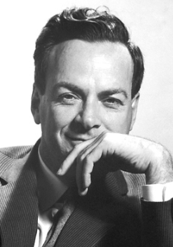
Richard Feynman gave a 1959 talk which many years later inspired the conceptual foundations of nanotechnology. https://handwiki.org/wiki/index.php?curid=78734
The American physicist Richard Feynman lectured, «There’s Plenty of Room at the Bottom,» at an American Physical Society meeting at Caltech on December 29, 1959, which is often held to have provided inspiration for the field of nanotechnology. Feynman had described a process by which the ability to manipulate individual atoms and molecules might be developed, using one set of precise tools to build and operate another proportionally smaller set, so on down to the needed scale. In the course of this, he noted, scaling issues would arise from the changing magnitude of various physical phenomena: gravity would become less important, surface tension and Van der Waals attraction would become more important.[6]
After Feynman’s death, a scholar studying the historical development of nanotechnology has concluded that his actual role in catalyzing nanotechnology research was limited, based on recollections from many of the people active in the nascent field in the 1980s and 1990s. Chris Toumey, a cultural anthropologist at the University of South Carolina, found that the published versions of Feynman’s talk had a negligible influence in the twenty years after it was first published, as measured by citations in the scientific literature, and not much more influence in the decade after the Scanning Tunneling Microscope was invented in 1981. Subsequently, interest in “Plenty of Room” in the scientific literature greatly increased in the early 1990s. This is probably because the term “nanotechnology” gained serious attention just before that time, following its use by K. Eric Drexler in his 1986 book, Engines of Creation: The Coming Era of Nanotechnology, which took the Feynman concept of a billion tiny factories and added the idea that they could make more copies of themselves via computer control instead of control by a human operator; and in a cover article headlined «Nanotechnology»,[7][8] published later that year in a mass-circulation science-oriented magazine, Omni. Toumey’s analysis also includes comments from distinguished scientists in nanotechnology who say that “Plenty of Room” did not influence their early work, and in fact most of them had not read it until a later date.[9][10]
These and other developments hint that the retroactive rediscovery of Feynman’s “Plenty of Room” gave nanotechnology a packaged history that provided an early date of December 1959, plus a connection to the charisma and genius of Richard Feynman. Feynman’s stature as a Nobel laureate and as an iconic figure in 20th century science surely helped advocates of nanotechnology and provided a valuable intellectual link to the past.[11]
2.2. Norio Taniguchi
The Japanese scientist called Norio Taniguchi of Tokyo University of Science was first to use the term «nano-technology» in a 1974 conference,[12] to describe semiconductor processes such as thin film deposition and ion beam milling exhibiting characteristic control on the order of a nanometer. His definition was, «‘Nano-technology’ mainly consists of the processing of, separation, consolidation, and deformation of materials by one atom or one molecule.» However, the term was not used again until 1981 when Eric Drexler, who was unaware of Taniguchi’s prior use of the term, published his first paper on nanotechnology in 1981.[13][14][15]
2.3. K. Eric Drexler
In the 1980s the idea of nanotechnology as a deterministic, rather than stochastic, handling of individual atoms and molecules was conceptually explored in depth by K. Eric Drexler, who promoted the technological significance of nano-scale phenomena and devices through speeches and two influential books.
In 1980, Drexler encountered Feynman’s provocative 1959 talk «There’s Plenty of Room at the Bottom» while preparing his initial scientific paper on the subject, “Molecular Engineering: An approach to the development of general capabilities for molecular manipulation,” published in the Proceedings of the National Academy of Sciences in 1981.[16] The term «nanotechnology» (which paralleled Taniguchi’s «nano-technology») was independently applied by Drexler in his 1986 book Engines of Creation: The Coming Era of Nanotechnology, which proposed the idea of a nanoscale «assembler» which would be able to build a copy of itself and of other items of arbitrary complexity. He also first published the term «grey goo» to describe what might happen if a hypothetical self-replicating machine, capable of independent operation, were constructed and released. Drexler’s vision of nanotechnology is often called «Molecular Nanotechnology» (MNT) or «molecular manufacturing.»
His 1991 Ph.D. work at the MIT Media Lab was the first doctoral degree on the topic of molecular nanotechnology and (after some editing) his thesis, «Molecular Machinery and Manufacturing with Applications to Computation,»[17] was published as Nanosystems: Molecular Machinery, Manufacturing, and Computation,[18] which received the Association of American Publishers award for Best Computer Science Book of 1992. Drexler founded the Foresight Institute in 1986 with the mission of «Preparing for nanotechnology.” Drexler is no longer a member of the Foresight Institute.
3. Experimental Research and Advances
In nanoelectronics, nanoscale thickness was demonstrated in the gate oxide and thin films used in transistors as early as the 1960s, but it was not until the late 1990s that MOSFETs (metal–oxide–semiconductor field-effect transistors) with nanoscale gate length were demonstrated. Nanotechnology and nanoscience got a boost in the early 1980s with two major developments: the birth of cluster science and the invention of the scanning tunneling microscope (STM). These developments led to the discovery of fullerenes in 1985 and the structural assignment of carbon nanotubes in 1991. The development of FinFET in the 1990s aldo laid the foundations for modern nanoelectronic semiconductor device fabrication.
3.1. Invention of Scanning Probe Microscopy
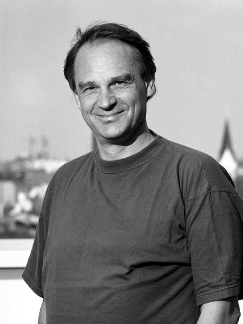
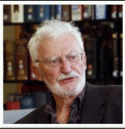
The scanning tunneling microscope, an instrument for imaging surfaces at the atomic level, was developed in 1981 by Gerd Binnig and Heinrich Rohrer at IBM Zurich Research Laboratory, for which they were awarded the Nobel Prize in Physics in 1986.[19][20] Binnig, Calvin Quate and Christoph Gerber invented the first atomic force microscope in 1986. The first commercially available atomic force microscope was introduced in 1989.
IBM researcher Don Eigler was the first to manipulate atoms using a scanning tunneling microscope in 1989. He used 35 Xenon atoms to spell out the IBM logo.[21] He shared the 2010 Kavli Prize in Nanoscience for this work.[22]
3.2. Advances in Interface and Colloid Science
Interface and colloid science had existed for nearly a century before they became associated with nanotechnology.[23][24] The first observations and size measurements of nanoparticles had been made during the first decade of the 20th century by Richard Adolf Zsigmondy, winner of the 1925 Nobel Prize in Chemistry, who made a detailed study of gold sols and other nanomaterials with sizes down to 10 nm using an ultramicroscope which was capable of visualizing particles much smaller than the light wavelength.[25] Zsigmondy was also the first to use the term «nanometer» explicitly for characterizing particle size. In the 1920s, Irving Langmuir, winner of the 1932 Nobel Prize in Chemistry, and Katharine B. Blodgett introduced the concept of a monolayer, a layer of material one molecule thick. In the early 1950s, Derjaguin and Abrikosova conducted the first measurement of surface forces.[26]
In 1974 the process of atomic layer deposition for depositing uniform thin films one atomic layer at a time was developed and patented by Tuomo Suntola and co-workers in Finland.[27]
In another development, the synthesis and properties of semiconductor nanocrystals were studied. This led to a fast increasing number of semiconductor nanoparticles of quantum dots.
3.3. Discovery of Fullerenes

Harry Kroto (left) won the 1996 Nobel Prize in Chemistry along with Richard Smalley (pictured below) and Robert Curl for their 1985 discovery of buckminsterfullerene, while Sumio Iijima (right) won the inaugural 2008 Kavli Prize in Nanoscience for his 1991 discovery of carbon nanotubes. https://handwiki.org/wiki/index.php?curid=1438073. https://handwiki.org/wiki/index.php?curid=1178382
Fullerenes were discovered in 1985 by Harry Kroto, Richard Smalley, and Robert Curl, who together won the 1996 Nobel Prize in Chemistry. Smalley’s research in physical chemistry investigated formation of inorganic and semiconductor clusters using pulsed molecular beams and time of flight mass spectrometry. As a consequence of this expertise, Curl introduced him to Kroto in order to investigate a question about the constituents of astronomical dust. These are carbon rich grains expelled by old stars such as R Corona Borealis. The result of this collaboration was the discovery of C60 and the fullerenes as the third allotropic form of carbon. Subsequent discoveries included the endohedral fullerenes, and the larger family of fullerenes the following year.[28][29]
The discovery of carbon nanotubes is largely attributed to Sumio Iijima of NEC in 1991, although carbon nanotubes have been produced and observed under a variety of conditions prior to 1991.[30] Iijima’s discovery of multi-walled carbon nanotubes in the insoluble material of arc-burned graphite rods in 1991[31] and Mintmire, Dunlap, and White’s independent prediction that if single-walled carbon nanotubes could be made, then they would exhibit remarkable conducting properties[32] helped create the initial buzz that is now associated with carbon nanotubes. Nanotube research accelerated greatly following the independent discoveries[33][34] by Bethune at IBM[35] and Iijima at NEC of single-walled carbon nanotubes and methods to specifically produce them by adding transition-metal catalysts to the carbon in an arc discharge.
In the early 1990s Huffman and Kraetschmer, of the University of Arizona, discovered how to synthesize and purify large quantities of fullerenes. This opened the door to their characterization and functionalization by hundreds of investigators in government and industrial laboratories. Shortly after, rubidium doped C60 was found to be a mid temperature (Tc = 32 K) superconductor. At a meeting of the Materials Research Society in 1992, Dr. T. Ebbesen (NEC) described to a spellbound audience his discovery and characterization of carbon nanotubes. This event sent those in attendance and others downwind of his presentation into their laboratories to reproduce and push those discoveries forward. Using the same or similar tools as those used by Huffman and Kratschmer, hundreds of researchers further developed the field of nanotube-based nanotechnology.
3.4. Nanoscale Transistors
A nanolayer-base metal–semiconductor junction (M–S junction) transistor was initially proposed and demonstrated by A. Rose in 1960, L. Geppert, Mohamed Atalla and Dawon Kahng in 1962.[36] Decades later, advances in multi-gate technology enabled the scaling of metal–oxide–semiconductor field-effect transistor (MOSFET) devices down to nano-scale levels smaller than 20 nm gate length, starting with the FinFET (fin field-effect transistor), a three-dimensional, non-planar, double-gate MOSFET. At UC Berkeley, a team of researchers including Digh Hisamoto, Chenming Hu, Tsu-Jae King Liu, Jeffrey Bokor and others fabricated FinFET devices down to a 17 nm process in 1998, then 15 nm in 2001, and then 10 nm in 2002.[37]
In 2006, a team of Korean researchers from the Korea Advanced Institute of Science and Technology (KAIST) and the National Nano Fab Center developed a 3 nm MOSFET, the world’s smallest nanoelectronic device. It was based on gate-all-around (GAA) FinFET technology.[38][39]
4. Government and Corporate Support
4.1. National Nanotechnology Initiative
Mihail Roco of the National Science Foundation formally proposed the National Nanotechnology Initiative to the White House, and was a key architect in its initial development. https://handwiki.org/wiki/index.php?curid=1506578
The National Nanotechnology Initiative is a United States federal nanotechnology research and development program. “The NNI serves as the central point of communication, cooperation, and collaboration for all Federal agencies engaged in nanotechnology research, bringing together the expertise needed to advance this broad and complex field.»[40] Its goals are to advance a world-class nanotechnology research and development (R&D) program, foster the transfer of new technologies into products for commercial and public benefit, develop and sustain educational resources, a skilled workforce, and the supporting infrastructure and tools to advance nanotechnology, and support responsible development of nanotechnology. The initiative was spearheaded by Mihail Roco, who formally proposed the National Nanotechnology Initiative to the Office of Science and Technology Policy during the Clinton administration in 1999, and was a key architect in its development. He is currently the Senior Advisor for Nanotechnology at the National Science Foundation, as well as the founding chair of the National Science and Technology Council subcommittee on Nanoscale Science, Engineering and Technology.[41]
President Bill Clinton advocated nanotechnology development. In a 21 January 2000 speech[42] at the California Institute of Technology, Clinton said, «Some of our research goals may take twenty or more years to achieve, but that is precisely why there is an important role for the federal government.» Feynman’s stature and concept of atomically precise fabrication played a role in securing funding for nanotechnology research, as mentioned in President Clinton’s speech:
My budget supports a major new National Nanotechnology Initiative, worth $500 million. Caltech is no stranger to the idea of nanotechnology the ability to manipulate matter at the atomic and molecular level. Over 40 years ago, Caltech’s own Richard Feynman asked, «What would happen if we could arrange the atoms one by one the way we want them?»[43]
President George W. Bush further increased funding for nanotechnology. On December 3, 2003 Bush signed into law the 21st Century Nanotechnology Research and Development Act,[44] which authorizes expenditures for five of the participating agencies totaling US$3.63 billion over four years.[45] The NNI budget supplement for Fiscal Year 2009 provides $1.5 billion to the NNI, reflecting steady growth in the nanotechnology investment.[46]
4.2. Other International Government and Corporate Support
Over sixty countries created nanotechnology research and development (R&D) government programs between 2001 and 2004. Government funding was exceeded by corporate spending on nanotechnology R&D, with most of the funding coming from corporations based in the United States, Japan and Germany. The top five organizations that filed the most intellectual patents on nanotechnology R&D between 1970 and 2011 were Samsung Electronics (2,578 first patents), Nippon Steel (1,490 first patents), IBM (1,360 first patents), Toshiba (1,298 first patents) and Canon (1,162 first patents). The top five organizations that published the most scientific papers on nanotechnology research between 1970 and 2012 were the Chinese Academy of Sciences, Russian Academy of Sciences, Centre national de la recherche scientifique, University of Tokyo and Osaka University.[47]
5. Growing Public Awareness and Controversy
5.1. «Why the Future doesn’t Need Us»
«Why the future doesn’t need us» is an article written by Bill Joy, then Chief Scientist at Sun Microsystems, in the April 2000 issue of Wired magazine. In the article, he argues that «Our most powerful 21st-century technologies — robotics, genetic engineering, and nanotech — are threatening to make humans an endangered species.» Joy argues that developing technologies provide a much greater danger to humanity than any technology before it has ever presented. In particular, he focuses on genetics, nanotechnology and robotics. He argues that 20th-century technologies of destruction, such as the nuclear bomb, were limited to large governments, due to the complexity and cost of such devices, as well as the difficulty in acquiring the required materials. He also voices concern about increasing computer power. His worry is that computers will eventually become more intelligent than we are, leading to such dystopian scenarios as robot rebellion. He notably quotes the Unabomber on this topic. After the publication of the article, Bill Joy suggested assessing technologies to gauge their implicit dangers, as well as having scientists refuse to work on technologies that have the potential to cause harm.
In the AAAS Science and Technology Policy Yearbook 2001 article titled A Response to Bill Joy and the Doom-and-Gloom Technofuturists, Bill Joy was criticized for having technological tunnel vision on his prediction, by failing to consider social factors.[48] In Ray Kurzweil’s The Singularity Is Near, he questioned the regulation of potentially dangerous technology, asking «Should we tell the millions of people afflicted with cancer and other devastating conditions that we are canceling the development of all bioengineered treatments because there is a risk that these same technologies may someday be used for malevolent purposes?».
5.2. Prey
Prey is a 2002 novel by Michael Crichton which features an artificial swarm of nanorobots which develop intelligence and threaten their human inventors. The novel generated concern within the nanotechnology community that the novel could negatively affect public perception of nanotechnology by creating fear of a similar scenario in real life.[49]
5.3. Drexler–Smalley Debate
Richard Smalley, best known for co-discovering the soccer ball-shaped “buckyball” molecule and a leading advocate of nanotechnology and its many applications, was an outspoken critic of the idea of molecular assemblers, as advocated by Eric Drexler. In 2001 he introduced scientific objections to them[50] attacking the notion of universal assemblers in a 2001 Scientific American article, leading to a rebuttal later that year from Drexler and colleagues,[51] and eventually to an exchange of open letters in 2003.[52]
Smalley criticized Drexler’s work on nanotechnology as naive, arguing that chemistry is extremely complicated, reactions are hard to control, and that a universal assembler is science fiction. Smalley believed that such assemblers were not physically possible and introduced scientific objections to them. His two principal technical objections, which he had termed the “fat fingers problem» and the «sticky fingers problem”, argued against the feasibility of molecular assemblers being able to precisely select and place individual atoms. He also believed that Drexler’s speculations about apocalyptic dangers of molecular assemblers threaten the public support for development of nanotechnology.
Smalley first argued that «fat fingers» made MNT impossible. He later argued that nanomachines would have to resemble chemical enzymes more than Drexler’s assemblers and could only work in water. He believed these would exclude the possibility of «molecular assemblers» that worked by precision picking and placing of individual atoms. Also, Smalley argued that nearly all of modern chemistry involves reactions that take place in a solvent (usually water), because the small molecules of a solvent contribute many things, such as lowering binding energies for transition states. Since nearly all known chemistry requires a solvent, Smalley felt that Drexler’s proposal to use a high vacuum environment was not feasible.
Smalley also believed that Drexler’s speculations about apocalyptic dangers of self-replicating machines that have been equated with «molecular assemblers» would threaten the public support for development of nanotechnology. To address the debate between Drexler and Smalley regarding molecular assemblers Chemical & Engineering News published a point-counterpoint consisting of an exchange of letters that addressed the issues.[52]
Drexler and coworkers responded to these two issues[51] in a 2001 publication. Drexler and colleagues noted that Drexler never proposed universal assemblers able to make absolutely anything, but instead proposed more limited assemblers able to make a very wide variety of things. They challenged the relevance of Smalley’s arguments to the more specific proposals advanced in Nanosystems. Drexler maintained that both were straw man arguments, and in the case of enzymes, Prof. Klibanov wrote in 1994, «…using an enzyme in organic solvents eliminates several obstacles…»[53] Drexler also addresses this in Nanosystems by showing mathematically that well designed catalysts can provide the effects of a solvent and can fundamentally be made even more efficient than a solvent/enzyme reaction could ever be. Drexler had difficulty in getting Smalley to respond, but in December 2003, Chemical & Engineering News carried a 4-part debate.[52]
Ray Kurzweil spends four pages in his book ‘The Singularity Is Near’ to showing that Richard Smalley’s arguments are not valid, and disputing them point by point. Kurzweil ends by stating that Drexler’s visions are very practicable and even happening already.[54]
5.4. Royal Society Report on the Implications of Nanotechnology
The Royal Society and Royal Academy of Engineering’s 2004 report on the implications of nanoscience and nanotechnologies[55] was inspired by Prince Charles’ concerns about nanotechnology, including molecular manufacturing. However, the report spent almost no time on molecular manufacturing.[56] In fact, the word «Drexler» appears only once in the body of the report (in passing), and «molecular manufacturing» or «molecular nanotechnology» not at all. The report covers various risks of nanoscale technologies, such as nanoparticle toxicology. It also provides a useful overview of several nanoscale fields. The report contains an annex (appendix) on grey goo, which cites a weaker variation of Richard Smalley’s contested argument against molecular manufacturing. It concludes that there is no evidence that autonomous, self replicating nanomachines will be developed in the foreseeable future, and suggests that regulators should be more concerned with issues of nanoparticle toxicology.
6. Initial Commercial Applications
The early 2000s saw the beginnings of the use of nanotechnology in commercial products, although most applications are limited to the bulk use of passive nanomaterials. Examples include titanium dioxide and zinc oxide nanoparticles in sunscreen, cosmetics and some food products; silver nanoparticles in food packaging, clothing, disinfectants and household appliances such as Silver Nano; carbon nanotubes for stain-resistant textiles; and cerium oxide as a fuel catalyst.[57] As of March 10, 2011, the Project on Emerging Nanotechnologies estimated that over 1300 manufacturer-identified nanotech products are publicly available, with new ones hitting the market at a pace of 3–4 per week.[58]
The National Science Foundation funded researcher David Berube to study the field of nanotechnology. His findings are published in the monograph Nano-Hype: The Truth Behind the Nanotechnology Buzz. This study concludes that much of what is sold as “nanotechnology” is in fact a recasting of straightforward materials science, which is leading to a “nanotech industry built solely on selling nanotubes, nanowires, and the like” which will “end up with a few suppliers selling low margin products in huge volumes.» Further applications which require actual manipulation or arrangement of nanoscale components await further research. Though technologies branded with the term ‘nano’ are sometimes little related to and fall far short of the most ambitious and transformative technological goals of the sort in molecular manufacturing proposals, the term still connotes such ideas. According to Berube, there may be a danger that a «nano bubble» will form, or is forming already, from the use of the term by scientists and entrepreneurs to garner funding, regardless of interest in the transformative possibilities of more ambitious and far-sighted work.[59]
Commercial nanoelectronic semiconductor device fabrication began in the 2010s. In 2013, SK Hynix began commercial mass-production of a 16 nm process,[60] TSMC began production of a 16 nm FinFET process,[61] and Samsung Electronics began production of a 10 nm process.[62] TSMC began production of a 7 nm process in 2017,[63] and Samsung began production of a 5 nm process in 2018.[64] In 2019, Samsung announced plans for the commercial production of a 3 nm GAAFET process by 2021.[65]
History of nanotechnology
|
Part of the article series on Nanotechnology |
|
History |
|
Subfields and related fields |
|
Nanomaterials |
|
Nanomedicine |
|
Molecular self-assembly |
|
Nanoelectronics |
|
Scanning probe microscopy |
|
Molecular nanotechnology This box: view • talk • edit |
Although nanotechnology is a relatively recent development in scientific research, the development of its central concepts happened over a longer period of time.
Additional recommended knowledge
Contents
- 1 Overview
- 2 Pre-Nanotechnology
- 3 Conceptual origins
- 4 Experimental advances
- 5 References
Overview
In 1965, Gordon Moore, one of the founders of Intel Corporation, made the astounding prediction that the number of transistors that could be fit in a given area would double every 18 months for the next ten years. This it did and the phenomenon became known as Moore’s Law. This trend has continued far past the predicted 10 years until this day, going from just over 2000 transistors in the original 4004 processors of 1971 to over 40,000,000 transistors in the Pentium 4. There has, of course, been a corresponding decrease in the size of individual electronic elements, going from millimeters in the 60’s to hundreds of nanometers in modern circuitry.
At the same time, the chemistry, biochemistry and molecular genetics communities have been moving in the other direction. Over much the same period, it has become possible to direct the synthesis, either in the test tube or in modified living organisms, of larger and larger and more and more complex molecular structures, up to tens or hundreds of nanometers in size. Enzymes are the molecular devices that drive life and in recent years it has both become possible to manipulate the structures and functions of these systems in vivo and to build complex biomimetic analogues in vitro.
Finally, the last quarter of a century has seen tremendous advances in our ability to control and manipulate light. Solid state lasers are now available for less than the price of a hamburger. We can generate light pulses as short as a few femtoseconds (1 fs = 10−15 s). We can image light with computers. And we can send information almost noiselessly along fiber optics at bandwidths of many gigabytes. Light too has a size and this size is also on the hundred nanometer scale.
Thus now, at the beginning of a new century, three powerful technologies have met on a common scale — the nanoscale — with the promise of revolutionizing both the worlds of electronics and of biology. This new field, which we refer to as biomolecular nanotechnology, holds many possibilities from fundamental research in molecular biology and biophysics to applications in biosensing, biocontrol, bioinformatics, genomics, medicine, computing, information storage and energy conversion.
Pre-Nanotechnology
Humans have unwittingly employed nanotechnology for thousands of years, for example in making steel and in vulcanizing rubber. Both of these processes rely on the properties of stochastically-formed atomic ensembles mere nanometers in size, and are distinguished from chemistry in that they don’t rely on the properties of individual molecules. But the development of the body of concepts now subsumed under the term nanotechnology has been slower.
The first mention of some of the distinguishing concepts in nanotechnology (but predating use of that name) was in 1867 by James Clerk Maxwell when he proposed as a thought experiment a tiny entity known as Maxwell’s Demon able to handle individual molecules.
The first observations and size measurements of nano-particles was made during first decade of 20th century. They are mostly associated with the name of Zsigmondy who made detail study of gold sols and other nanomaterials with sizes down to 10 nm and less. He published a book in 1914. [1]. He used ultramicroscope that employes dark field method for seeing particles with sizes much less than light wavelength. Zsigmondy was also the first who used nanometer explicitly for characterizing particle size. He determined it as 1/1,000,000 of millimeter. He developed a first system classification based on particle size in nanometer range.
There have been many significant developments during 20th century in characterizing nanomaterials and related phenomena, belonging to the field of interface and colloid science. In the 1920s, Irving Langmuir and Katharine B. Blodgett introduced the concept of a monolayer, a layer of material one molecule thick. Langmuir won a Nobel Prize in chemistry for his work. In early 1950s, Derjaguin and Abrikosova conducted the first measurement of surface forces [2].
There have been many studies of periodic colloidal structures and principles of molecular self-assembly that are overviewed in the paper [3]. There are many other discoveries that serve as scientific basis for the modern nanotechnology can be found in the «Fundamentals of Interface and Colloid Science by H.Lyklema [4].
Conceptual origins
The topic of nanotechnology was again touched upon by «There’s Plenty of Room at the Bottom,» a talk given by physicist Richard Feynman at an American Physical Society meeting at Caltech on December 29, 1959. Feynman described a process by which the ability to manipulate individual atoms and molecules might be developed, using one set of precise tools to build and operate another proportionally smaller set, so on down to the needed scale. In the course of this, he noted, scaling issues would arise from the changing magnitude of various physical phenomena: gravity would become less important, surface tension and Van der Waals attraction would become more important, etc. This basic idea appears feasible, and exponential assembly enhances it with parallelism to produce a useful quantity of end products. At the meeting, Feynman announced two challenges, and he offered a prize a $1000 for the first individuals to solve each one. The first challenge involved the construction of a nanomotor, which, to Feynman’s surprise, was achieved by November of 1960 by William McLellan. The second challenge involved the possibility of scaling down letters small enough so as to be able to fit the entire Encyclopedia Britannica on the head of a pin; this prize was claimed in 1985 by Tom Newman.[5]
In 1965 Gordon Moore observed that silicon transistors were undergoing a continual process of scaling downward, an observation which was later codified as Moore’s law. Since his observation transistor minimum feature sizes have decreased from 10 micrometers to the 45-65 nm range in 2007; one minimum feature is thus roughly 180 silicon atoms long
The term «nanotechnology» was first defined by Tokyo Science University, Norio Taniguchi in a 1974 paper (N. Taniguchi, «On the Basic Concept of ‘Nano-Technology’,» Proc. Intl. Conf. Prod. Eng. Tokyo, Part II, Japan Society of Precision Engineering, 1974.) as follows: «‘Nano-technology’ mainly consists of the processing of, separation, consolidation, and deformation of materials by one atom or one molecule.» Since that time the definition of nanotechnology has generally been extended upward in size to include features as large as 100 nm. Additionally, the idea that nanotechnology embraces structures exhibiting quantum mechanical aspects, such as quantum dots, has been thrown into the definition.
Also in 1974 the process of atomic layer deposition, for depositing uniform thin films one atomic layer at a time, was developed and patented by Dr. Tuomo Suntola and co-workers in Finland.
In the 1980s the idea of nanotechnology as deterministic, rather than stochastic, handling of individual atoms and molecules was conceptually explored in depth by Dr. K. Eric Drexler, who promoted the technological significance of nano-scale phenomena and devices through speeches and the books Engines of Creation: The Coming Era of Nanotechnology and Nanosystems: Molecular Machinery, Manufacturing, and Computation, (ISBN 0-471-57518-6). Drexler’s vision of nanotechnology is often called «Molecular Nanotechnology» (MNT) or «molecular manufacturing,» and Drexler at one point proposed the term «zettatech» which never became popular.
Experimental advances
Nanotechnology and nanoscience got a boost in the early 1980s with two major developments: the birth of cluster science and the invention of the scanning tunneling microscope (STM). This development led to the discovery of fullerenes in 1985 and the structural assignment of carbon nanotubes a few years later. In another development, the synthesis and properties of semiconductor nanocrystals were studied. This led to a fast increasing number of semiconductor nanoparticles of quantum dots.
In the early 1990s Huffman and Kraetschmer (U. Arizona) discovered how to synthesize and purify large quantities of fullerenes. This opened the door to their characterization and functionalization by hundreds of investigators in government and industrial laboratories. Shortly after, rubidium doped C60 was found to be a mid temperature (Tc = 32 K) superconductor. At a meeting of the Materials Research Society meeting in 1992, Dr. T. Ebbesen (NEC) described to a spellbound audience his discovery and characterization of carbon nanotubes. This event sent those in attendance and others downwind of his presentation into their laboratories to reproduce and push those discoveries forward. Using the same or similar tools as those used by Huffman and Kratschmere, hundreds of researchers further developed the field of nanotube-based nanotechnology.
At present in 2007 the practice of nanotechnology embraces both stochastic approaches (in which, for example, supramolecular chemistry creates waterproof pants) and deterministic approaches wherein single molecules (created by stochastic chemistry) are manipulated on substrate surfaces (created by stochastic deposition methods) by deterministic methods comprising nudging them with STM or AFM probes and causing simple binding or cleavage reactions to occur. The dream of a complex, deterministic molecular nanotechnology remains elusive. Since the mid 1990s, thousands of surface scientists and thin film technocrats have latched on to the nanotechnology bandwagon and redefined their disciplines as nanotechnology. This has caused much confusion in the field and has spawned thousands of «nano»-papers on the peer reviewed literature. Most of these reports are extensions of the more ordinary research done in the parent fields.
For the future, some means has to be found for MNT design evolution at the nanoscale which mimics the process of biological evolution at the molecular scale. Biological evolution proceeds by random variation in ensemble averages of organisms combined with culling of the less-successful variants and reproduction of the more-successful variants, and macroscale engineering design also proceeds by a process of design evolution from simplicity to complexity as set forth somewhat satirically by John Gall: «A complex system that works is invariably found to have evolved from a simple system that worked. . . . A complex system designed from scratch never works and can not be patched up to make it work. You have to start over, beginning with a system that works.» [6] A breakthrough in MNT is needed which proceeds from the simple atomic ensembles which can be built with, e.g., an STM to complex MNT systems via a process of design evolution. A handicap in this process is the difficulty of seeing and manipulation at the nanoscale compared to the macroscale which makes deterministic selection of successful trials difficult; in contrast biological evolution proceeds via action of what Richard Dawkins has called the «blind watchmaker»
[7]
comprising random molecular variation and deterministic reproduction/extinction.
References
- ^ Zsigmondy, R. «Colloids and the Ultramicroscope», J.Wiley and Sons, NY, (1914)
- ^ Derjaguin, B.V. Discuss. Faraday Soc., No. 18, 24-27, 182-187, 198, 211, 215-219 (1954)
- ^ Efremov, I.F. «Periodic Colloidal Structures», in «Surface and Colloid Science», vol. 8, Wiley, NY (1975)
- ^ Lyklema, J. «Fundamentals of Interface and Colloid Science», vol.1-5 Academic Press, (1995-2000)
- ^ Gribbin, John. «Richard Feynman: A Life in Science» Dutton 1997, pg 170.
- ^
Gall, John, (1986) Systemantics: How Systems Really Work and How They Fail, 2nd ed. Ann Arbor, MI : The General Systemantics Press. - ^
Richard Dawkins, The Blind Watchmaker: Why the Evidence of Evolution Reveals a Universe Without Design, W. W. Norton; Reissue edition (September 19, 1996)
Traditionally, the origins of nanotechnology are traced back to December 29, 1959, when Professor Richard Feynman (a 1965 Nobel Prize winner in physics) presented a lecture entitled “There’s Plenty of Room at the Bottom” during the annual meeting of the American Physical Society at the California Institute of Technology (Caltech). In this talk, Feynman spoke about the principles of miniaturization and atomic-level precision and how these concepts do not violate any known law of physics. Feynman described a process by which the ability to manipulate individual atoms and molecules might be developed, using one set of precise tools to build and operate another proportionally smaller set, and so on down to the needed scale.
He described a field that few researchers had thought much about, let alone investigated. Feynman presented the idea of manipulating and controlling things on an extremely small scale by building and shaping matter one atom at a time. He proposed that it was possible to build a surgical nanoscale robot by developing quarter-scale manipulator hands that would build quarter-scale machine tools analogous to those found in machine shops, continuing until the nanoscale is reached, eight iterations later.
|
|
|
Richard Feynman |

He described how the 24 volumes of the Encyclopedia Britannica could be written on the head of a pin. He imagined raised letters of black metal that could be reduced to 1/25,000 of their normal size (the size of this type). Feynman discussed how such a work could be read using an electron microscope in use at that time. The trick, he said, was to write the super small texts and scale them down without loss of resolution.
Feynman also discussed systems in nature that achieve atomic-level precision unaided by human design. Furthermore, he laid out some precise steps that might need to be taken in order to begin work in this uncharted field. These included the development of more powerful electron microscopes, key tools in viewing the very small. He also discussed the need for more fundamental discovery in biology and biochemistry.
The term «nanotechnology» was defined by Tokyo University of Science Professor Norio Taniguchi, in a 1974 paper entitled “On the Basic Concept of ‘Nano-Technology’, as follows: ‘Nanotechnology’ mainly consists of the processing of, separation, consolidation, and deformation of materials by one atom or by one molecule.» In his paper, Taniguchi developed Feynman’s ideas in more detail stating that “Nano-technology is the production technology to get the extra high accuracy and ultra-fine dimensions, i.e., the preciseness and fineness of the order of 1 nm (nanometer) in length. He also discussed his concept of ‘nanotechnology’ in materials processing, basing this on the microscopic behavior of materials.
|
|
|
Norio Taniguchi |

The main step in the development of nanotechnology was the invention of cluster science and Scanning Tunneling Microscope (STM) in the 1980’s. In 1981, Gerd Binnig and Heinrich Rohrer of IBM’s Zurich Research Laboratory created the STM that allowed scientists to see and move individual atoms for the first time. They found that by using an electrical field and a special nanoprobe with a super small tip, they could move atoms around into forms that they wanted.
 |
| Scanning Tunneling Microscope block diagram (Wikipedia) |
In September 1985, a new kind of carbon (C60) was discovered by three innovative chemists, who came together at Rice University in Houston, Texas, to perform a set of experiments that changed chemistry and the world. The new carbon family was named the fullerenes. The fullerenes—soccer ball shaped, cage-like molecules, characterized by the symmetrical C60—soon occupied center stage in chemistry. Very different from known carbon forms like graphite and diamond, C60 (made up of 60 carbons) was officially named Buckminster fullerene (also called the buckyball). The buckyball was so named because of the resemblance to the geodesic domes that the architect Richard Buckminster Fuller popularized.
|
|
|
Buckminster fullerene (Wikipedia) |

The basic ideas is this field were popularized and explored in much more depth in the 1980’s, when K. Eric Drexler promoted the technological significance of nano-scale phenomena and devices through speeches and the books Engines of Creation: The Coming Era of Nanotechnology (1986) and Nanosystems: Molecular Machinery, Manufacturing, and Computation.
|
|
|
K. Eric Drexler |

He talked about building machines on the scale of molecules, a few nanometers wide—motors, robot arms, and even whole computers, far smaller than a cell. Drexler spent the most of his time ever since describing and analyzing these incredible devices, and responding to accusations of science fiction.

Aimed at a non-technical audience while also appealing to scientists, Drexler’s book was a highly original work describing a new form of technology based on molecular “assemblers,” which would be able to “place atoms in almost any reasonable arrangement” and thereby allow the formation of “almost anything the laws of nature allow.” This may sound like a fanciful and fantastical idea but, as Drexler points out, this is something that nature already does, unaided by human design, with the biologically based machines inside our own bodies (and those of any biological species).
Another of the defining moments in nanotechnology came in 1989 when Don Eigler used a SPM at the IBM Almaden Research Center in San Jose, California to spell out the letters IBM from 35 xenon atoms and photographed his success. For the first time we could put atoms exactly where we wanted them, even if keeping them there at much above absolute zero proved to be a problem. While useful in aiding our understanding of the nanoworld, arranging atoms together one by one is unlikely to be of much use in industrial processes.
|
|
|
IBM logo spelled out using 35 xenon atoms |

The first commercially available Atomic Force Microscope (AFM) or Scanning Force Microscope (SFM) was also introduced in 1989 and that is still a very powerful tool to work on the nanoscale.
|
|
|
Atomic Force Microscope block diagram (Wikipedia) |

In 1991, nanoscale materials became the focus of intense research with the discovery of the carbon nanotubes Sumio Iijima at NEC Fundamental Research Laboratories in Tsukuba, Japan.
|
|
|
Sumio Iijima |

Iijima’s high-resolution multi-walled carbon nanotube (MWNT) electron micrographs illustrated that the new carbon species with rounded end caps were fullerene cousins.
|
|
|
Multi-Walled Carbon Nanotube |

But while MWNTs are related to fullerenes, they were not molecularly perfect. However, the single-walled carbon nanotubes (SWNTs) discovered in 1993, simultaneously by Iijima and Toshinari Ichihashi at NEC in Japan and Donald S. Bethune and others at IBM Almaden Research Center in San Jose, California, were different.
|
|
|
Single-Walled Carbon Nanotubes |

Since then, new discoveries in this field are happening almost on a daily basis…
Nanotechnology
is the science that studies the use of matter on a nanometric scale. The
history of nanotechnology has its beginning in the speech that Richard Feynman
gave at the University of Caltech (California). In this famous speech, Feynman was
the first to talk about nanotechnology, nanoscience and about all the
possibilities it offers. Today, the field of nanotechnology is in full growth
and has high hopes that are waiting to be fulfilled. This article describes in
detail the history of Nanotechnology, its importance, applications, trends, and
the future.
Nano has been
the most heard word in recent years in science fiction films and also in the
media in connection with food or other products. But what exactly is
nanotechnology, and who came up with the idea of researching the properties
of tiny particles and how was it discovered?
The term
nanotechnology describes all areas of research in the field of single atoms up
to structural sizes of 100 nanometers or less. One nanometer equals one-billionth
of a meter. The peculiarities of research in the nanoscale represent the
altered properties of the objects in this size range. Volume properties take a
back seat to the laws of quantum physics and thus allow unprecedented effects.
Nanotechnology is now used in all technological research areas. These include,
for example, the chemical industry, the semiconductor industry, mechanical
engineering, and food technology.
The origin of
Nanotechnology
The
nanotechnology that has become so popular in the last decade has its origin
back in 1959 when the American physicist and later Nobel laureate gave the
lecture «There’s Plenty of Room at the Bottom». In it, he dealt with
the possible influence of molecules of the order of atoms. The term nanotechnology
itself was first used by the Japanese professor Norio Taniguchi in 1974 in a
contribution to semiconductor processes and possible applications. The
imagination thus aroused by the researchers finally led to the development of
the scanning tunneling microscope in 1981, for which the physicists Binning and
Rohrer were awarded the Nobel Prize in 1986.
Nanotechnology
deals with the manipulation of matter at the size of 10-9 nm. Scientists did
not consider its importance until Richard Feynman gave his speech, although, in
some occasions in laboratories, they managed to create an atomic level compound
with properties similar to those of current nanotechnology. In fact, the
popular belief is that at some point in history, graphene sheets and nanotubes were
manufactured that are so popular today.
In the past,
nanotechnology was not studied until several books were published talking about
it and its potential. Richard Feynman’s famous phrase «there is a lot of
space in the background» made him an iconic figure of the twentieth
century and made many other scientists interested in nanotechnology.
At the time of
the speech of Feynman, many scientific fields seemed to have reached a point of
stagnation and Richard Feynman was the first to venture to say that in the
smallest (atomic level), there is a science that could give great results. He
proposed the example of the human body, in which the manipulation of atoms and
life cells (DNA) that are of great importance in the functioning of the
organism could be interesting. Its correct use could give the solution to many
problems and could be very useful in the development of cures for future
diseases.
The scanning
tunneling microscope then allowed the rapid gain of experience in the field of
quantum mechanics. At the end of the 1980s and early 1990s, the scientist Eric
Drexler developed revolutionary ideas for the creation and construction of
complex machines and materials made of single atoms. These visions have
motivated many scientists since then to deal critically with the history and
development of nanotechnology and the associated possibilities. Source
Applications
of Nanotechnology
Thanks to
improved materials and surfaces, nanotechnology is now improving the
performance of medical diagnostic and therapeutic devices, textiles, household
appliances and, not least, communication technologies. For the consumer, it is
difficult to see where the nanoparticles are used. The lotus effect is certainly an important aspect. Self-cleaning surfaces improve the cleaning
of car paints or windows. The additives on which these coatings are based are
also used in paints and roof tiles, for example, in order to delay the
weathering and aging for as long as possible.
But in many
other things of everyday life, there is nanotechnology. Waterproof
nanoparticle-clad clothing, sunscreens with active ingredients to enhance UV
protection, and edible oil with nanoparticle-packed vitamins are just a few
examples. Finished soups and table salt trickle out of the packaging thanks to
nanotechnology. The cosmetics industry also uses nanoparticles to develop
previously unknown properties in creams and powders.
Today, the
sports industry manufactures ultra-light tennis rackets, skis or bicycles with
improved materials. Golf balls allow a more precise game due to the
nano-coating and the associated improvement in-flight characteristics.
Tires are more
resistant thanks to the use of nanoparticles and the rolling properties are
improved. This extends the life and contributes to a reduced fuel requirement.
Smaller and
smaller cell phones and computers are also partly due to the use of nanotechnology
and its success story. The ever-better quality of the lighting of displays in
navigation devices or smartphones is directly dependent on optimized nano-sized
light sources.
This overview
clearly shows that in the meantime, there are many applications in all areas of
life — and new ones are added every week. Source
Read: 60 Uses of Graphene — The Ultimate Guide to Graphene’s (Potential) Applications in 2019
Trends in
Nanotechnology
Nanotechnology
opens up an almost unlimited field of research activity. Especially in
medicine, nanotechnology offers exciting opportunities. Novel diagnostic
procedures and therapies promise wide-ranging development potential. For example,
novel drugs can be developed. Supported by the progressive miniaturization in
the electronics industry, interdisciplinary research teams are researching
so-called nanobots. Prototypes already available today should continue to
shrink below the size of blood cells and be able to move in the human organism.
These nanobots could then transport drugs and dose them specifically to the
disease centers.
The development
of long fibrous devices that can be introduced into the human organism would be
the consequent continuation of minimally invasive surgery. Substances could be
more specifically administered and, for example, tissue samples.
Classic
mechanical and plant engineering also wants to benefit from innovative
materials whose structures show improved properties during machining and in
use. So today the rotors of wind turbines are designed with a special coating,
which has a positive effect on efficiency.
The ever-focused
area of power generation and storage is developing new systems to quench the
hunger for energy from previously unused sources. Novel concepts for energy
generation, for example from ambient temperature or air movement combined with
the optimized capacity of the storage media, promise a more efficient use of
the energy available in nature.
The food
industry is researching foods that, for example, have a longer shelf life due
to the nanoparticles or, depending on their temperature and duration, have
different flavors in the domestic oven. But also in agriculture, nanotechnology
is used for developments in the field of biological crop protection.
Critical
voices
At the end of
the 1990s, enthusiasm for the new technology was mixed with critical voices
warning of the dangers. Various studies and publications highlighted possible
effects from different perspectives. However, given the limitations of human
knowledge about future developments and the associated potentials, no generally
accepted recommendations can be made. In particular, the impact of nanoparticle
uptake into living things has made critics cry out. Although enrichment of the
particles does not necessarily mean damage to the organisms, uncertainty
remains in view of the hitherto sparse long-term experience.
Critics expressed
concerns that nanoparticles, like asbestos, could have a negative impact on
humans. A few years ago, American researchers from the University of
Massachusetts published a study showing that nanoparticles can damage DNA and
trigger the development of cancer. They recommend high safety standards for the
manufacturing processes and warn against contamination of the environment with
the nanoparticles. As a consequence, insurance companies limit the maximum
amount of cover for insurance contracts in nanotechnology. They demand
international safety standards.
The positive
development opportunities offered by the use of nanotechnology are counteracted
by the hitherto unanswered questions about the dangers and risks. It is
therefore important to develop nanotechnology in a social context. The Government
of Germany, therefore, created Nanokommission in 2008. It is made up of
representatives from business, consumer protection, and nature conservation
associations as well as representatives from various ministries, bringing
together the most important stakeholders. The Commission is concerned with
potential opportunities as well as nanotechnology risks to the environment and
health. In various working groups, detailed questions on consumer and
environmental protection are discussed.
Future of Nanotechnology
Nanotechnology is often referred to as «the future technology» that can solve
many problems. Some even talk about a nanotechnology revolution. Nanotechnology
definitely brings tremendous benefits and potential, but the fact that even the
youngest technology has its dangers, and much less explored, should be well
known to everyone.
It is claimed
that environmental problems such as pollution and climate change could also be
solved. However, there are also negative properties that nanotechnology
entails. For example, the development of usable nanoparticles requires enormous
energy and water consumption as well as the use of toxic solvents and
chemicals. In addition, the use of nano packaging promotes longer shelf life of
food, which in turn means that the food continues to be transported over long
distances. Everyone knows that global transport is a major environmental
burden. For humans, dangers arise when such nano-pesticides are ingested via
food, as research cannot yet foresee how the human body absorbs and degrades
these substances. Source

In conclusion, Nanotechnology
has now gone well beyond the scope of science fiction stories. Nanotechnologies
are now mainly interested in the composition of materials, but their potential
applications go far beyond. Nanotechnology has seen a prosperous growth, it is
well used and can be fundamental in the near future. It has caused a positive
impact on life in the sectors of medicine, food, energy that could change our
lives which makes it worthy of a science fiction story. This has become
possible only due to the revolutionary speech of Richard Feynman as he led the
foundation of this industry and motivated others to explore this technology. In
the future, much more advanced applications of nanotechnology are expected due
to their unique characteristics.
7th Nov 2019