
From Wikipedia, the free encyclopedia
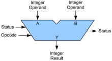
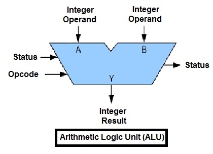
A symbolic representation of an ALU and its input and output signals, indicated by arrows pointing into or out of the ALU, respectively. Each arrow represents one or more signals. Control signals enter from the left and status signals exit on the right; data flows from top to bottom.
In computing, an arithmetic logic unit (ALU) is a combinational digital circuit that performs arithmetic and bitwise operations on integer binary numbers.[1][2][3] This is in contrast to a floating-point unit (FPU), which operates on floating point numbers. It is a fundamental building block of many types of computing circuits, including the central processing unit (CPU) of computers, FPUs, and graphics processing units (GPUs).[4]
The inputs to an ALU are the data to be operated on, called operands, and a code indicating the operation to be performed; the ALU’s output is the result of the performed operation. In many designs, the ALU also has status inputs or outputs, or both, which convey information about a previous operation or the current operation, respectively, between the ALU and external status registers.
Signals[edit]
An ALU has a variety of input and output nets, which are the electrical conductors used to convey digital signals between the ALU and external circuitry. When an ALU is operating, external circuits apply signals to the ALU inputs and, in response, the ALU produces and conveys signals to external circuitry via its outputs.
Data[edit]
A basic ALU has three parallel data buses consisting of two input operands (A and B) and a result output (Y). Each data bus is a group of signals that conveys one binary integer number. Typically, the A, B and Y bus widths (the number of signals comprising each bus) are identical and match the native word size of the external circuitry (e.g., the encapsulating CPU or other processor).
Opcode[edit]
The opcode input is a parallel bus that conveys to the ALU an operation selection code, which is an enumerated value that specifies the desired arithmetic or logic operation to be performed by the ALU. The opcode size (its bus width) determines the maximum number of distinct operations the ALU can perform; for example, a four-bit opcode can specify up to sixteen different ALU operations. Generally, an ALU opcode is not the same as a machine language opcode, though in some cases it may be directly encoded as a bit field within a machine language opcode.
Status[edit]
Outputs[edit]
The status outputs are various individual signals that convey supplemental information about the result of the current ALU operation. General-purpose ALUs commonly have status signals such as:
- Carry-out, which conveys the carry resulting from an addition operation, the borrow resulting from a subtraction operation, or the overflow bit resulting from a binary shift operation.
- Zero, which indicates all bits of Y are logic zero.
- Negative, which indicates the result of an arithmetic operation is negative.
- Overflow, which indicates the result of an arithmetic operation has exceeded the numeric range of Y.
- Parity, which indicates whether an even or odd number of bits in Y are logic one.
Upon completion of each ALU operation, the status output signals are usually stored in external registers to make them available for future ALU operations (e.g., to implement multiple-precision arithmetic) or for controlling conditional branching. The collection of bit registers that store the status outputs are often treated as a single, multi-bit register, which is referred to as the «status register» or «condition code register».
Inputs[edit]
The status inputs allow additional information to be made available to the ALU when performing an operation. Typically, this is a single «carry-in» bit that is the stored carry-out from a previous ALU operation.
Circuit operation[edit]
An ALU is a combinational logic circuit, meaning that its outputs will change asynchronously in response to input changes. In normal operation, stable signals are applied to all of the ALU inputs and, when enough time (known as the «propagation delay») has passed for the signals to propagate through the ALU circuitry, the result of the ALU operation appears at the ALU outputs. The external circuitry connected to the ALU is responsible for ensuring the stability of ALU input signals throughout the operation, and for allowing sufficient time for the signals to propagate through the ALU before sampling the ALU result.
In general, external circuitry controls an ALU by applying signals to its inputs. Typically, the external circuitry employs sequential logic to control the ALU operation, which is paced by a clock signal of a sufficiently low frequency to ensure enough time for the ALU outputs to settle under worst-case conditions.
For example, a CPU begins an ALU addition operation by routing operands from their sources (which are usually registers) to the ALU’s operand inputs, while the control unit simultaneously applies a value to the ALU’s opcode input, configuring it to perform addition. At the same time, the CPU also routes the ALU result output to a destination register that will receive the sum. The ALU’s input signals, which are held stable until the next clock, are allowed to propagate through the ALU and to the destination register while the CPU waits for the next clock. When the next clock arrives, the destination register stores the ALU result and, since the ALU operation has completed, the ALU inputs may be set up for the next ALU operation.
Functions[edit]
A number of basic arithmetic and bitwise logic functions are commonly supported by ALUs. Basic, general purpose ALUs typically include these operations in their repertoires:[1][2][3][5]
Arithmetic operations[edit]
- Add: A and B are summed and the sum appears at Y and carry-out.
- Add with carry: A, B and carry-in are summed and the sum appears at Y and carry-out.
- Subtract: B is subtracted from A (or vice versa) and the difference appears at Y and carry-out. For this function, carry-out is effectively a «borrow» indicator. This operation may also be used to compare the magnitudes of A and B; in such cases the Y output may be ignored by the processor, which is only interested in the status bits (particularly zero and negative) that result from the operation.
- Subtract with borrow: B is subtracted from A (or vice versa) with borrow (carry-in) and the difference appears at Y and carry-out (borrow out).
- Two’s complement (negate): A (or B) is subtracted from zero and the difference appears at Y.
- Increment: A (or B) is increased by one and the resulting value appears at Y.
- Decrement: A (or B) is decreased by one and the resulting value appears at Y.
- Pass through: all bits of A (or B) appear unmodified at Y. This operation is typically used to determine the parity of the operand or whether it is zero or negative, or to load the operand into a processor register.
Bitwise logical operations[edit]
- AND: the bitwise AND of A and B appears at Y.
- OR: the bitwise OR of A and B appears at Y.
- Exclusive-OR: the bitwise XOR of A and B appears at Y.
- Ones’ complement: all bits of A (or B) are inverted and appear at Y.
Bit shift operations[edit]
| Type | Left | Right |
|---|---|---|
| Arithmetic shift | 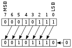
|

|
| Logical shift |
|
|
| Rotate | 
|
|
| Rotate through carry | 
|

|
ALU shift operations cause operand A (or B) to shift left or right (depending on the opcode) and the shifted operand appears at Y. Simple ALUs typically can shift the operand by only one bit position, whereas more complex ALUs employ barrel shifters that allow them to shift the operand by an arbitrary number of bits in one operation. In all single-bit shift operations, the bit shifted out of the operand appears on carry-out; the value of the bit shifted into the operand depends on the type of shift.
- Arithmetic shift: the operand is treated as a two’s complement integer, meaning that the most significant bit is a «sign» bit and is preserved.
- Logical shift: a logic zero is shifted into the operand. This is used to shift unsigned integers.
- Rotate: the operand is treated as a circular buffer of bits so its least and most significant bits are effectively adjacent.
- Rotate through carry: the carry bit and operand are collectively treated as a circular buffer of bits.
Applications[edit]
Multiple-precision arithmetic[edit]
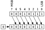
In integer arithmetic computations, multiple-precision arithmetic is an algorithm that operates on integers which are larger than the ALU word size. To do this, the algorithm treats each operand as an ordered collection of ALU-size fragments, arranged from most-significant (MS) to least-significant (LS) or vice versa. For example, in the case of an 8-bit ALU, the 24-bit integer 0x123456 would be treated as a collection of three 8-bit fragments: 0x12 (MS), 0x34, and 0x56 (LS). Since the size of a fragment exactly matches the ALU word size, the ALU can directly operate on this «piece» of operand.
The algorithm uses the ALU to directly operate on particular operand fragments and thus generate a corresponding fragment (a «partial») of the multi-precision result. Each partial, when generated, is written to an associated region of storage that has been designated for the multiple-precision result. This process is repeated for all operand fragments so as to generate a complete collection of partials, which is the result of the multiple-precision operation.
In arithmetic operations (e.g., addition, subtraction), the algorithm starts by invoking an ALU operation on the operands’ LS fragments, thereby producing both a LS partial and a carry out bit. The algorithm writes the partial to designated storage, whereas the processor’s state machine typically stores the carry out bit to an ALU status register. The algorithm then advances to the next fragment of each operand’s collection and invokes an ALU operation on these fragments along with the stored carry bit from the previous ALU operation, thus producing another (more significant) partial and a carry out bit. As before, the carry bit is stored to the status register and the partial is written to designated storage. This process repeats until all operand fragments have been processed, resulting in a complete collection of partials in storage, which comprise the multi-precision arithmetic result.
In multiple-precision shift operations, the order of operand fragment processing depends on the shift direction. In left-shift operations, fragments are processed LS first because the LS bit of each partial—which is conveyed via the stored carry bit—must be obtained from the MS bit of the previously left-shifted, less-significant operand. Conversely, operands are processed MS first in right-shift operations because the MS bit of each partial must be obtained from the LS bit of the previously right-shifted, more-significant operand.
In bitwise logical operations (e.g., logical AND, logical OR), the operand fragments may be processed in any arbitrary order because each partial depends only on the corresponding operand fragments (the stored carry bit from the previous ALU operation is ignored).
Complex operations[edit]
Although an ALU can be designed to perform complex functions, the resulting higher circuit complexity, cost, power consumption and larger size makes this impractical in many cases. Consequently, ALUs are often limited to simple functions that can be executed at very high speeds (i.e., very short propagation delays), and the external processor circuitry is responsible for performing complex functions by orchestrating a sequence of simpler ALU operations.
For example, computing the square root of a number might be implemented in various ways, depending on ALU complexity:
- Calculation in a single clock: a very complex ALU that calculates a square root in one operation.
- Calculation pipeline: a group of simple ALUs that calculates a square root in stages, with intermediate results passing through ALUs arranged like a factory production line. This circuit can accept new operands before finishing the previous ones and produces results as fast as the very complex ALU, though the results are delayed by the sum of the propagation delays of the ALU stages. For more information, see the article on instruction pipelining.
- Iterative calculation: a simple ALU that calculates the square root through several steps under the direction of a control unit.
The implementations above transition from fastest and most expensive to slowest and least costly. The square root is calculated in all cases, but processors with simple ALUs will take longer to perform the calculation because multiple ALU operations must be performed.
Implementation[edit]
An ALU is usually implemented either as a stand-alone integrated circuit (IC), such as the 74181, or as part of a more complex IC. In the latter case, an ALU is typically instantiated by synthesizing it from a description written in VHDL, Verilog or some other hardware description language. For example, the following VHDL code describes a very simple 8-bit ALU:
entity alu is
port (  -- the alu connections to external circuitry:
  A  : in signed(7 downto 0);   -- operand A
  B  : in signed(7 downto 0);   -- operand B
  OP : in unsigned(2 downto 0); -- opcode
  Y  : out signed(7 downto 0));  -- operation result
end alu;

architecture behavioral of alu is
begin
 case OP is  -- decode the opcode and perform the operation:
 when "000" =>  Y <= A + B;   -- add
 when "001" =>  Y <= A - B;   -- subtract
 when "010" =>  Y <= A - 1;   -- decrement
 when "011" =>  Y <= A + 1;   -- increment
 when "100" =>  Y <= not A;   -- 1's complement
 when "101" =>  Y <= A and B; -- bitwise AND
 when "110" =>  Y <= A or B;  -- bitwise OR
 when "111" =>  Y <= A xor B; -- bitwise XOR
 when others => Y <= (others => 'X');
 end case;
end behavioral;
History[edit]
Mathematician John von Neumann proposed the ALU concept in 1945 in a report on the foundations for a new computer called the EDVAC.[6]
The cost, size, and power consumption of electronic circuitry was relatively high throughout the infancy of the information age. Consequently, all serial computers and many early computers, such as the PDP-8, had a simple ALU that operated on one data bit at a time, although they often presented a wider word size to programmers. One of the earliest computers to have multiple discrete single-bit ALU circuits was the 1948 Whirlwind I, which employed sixteen such «math units» to enable it to operate on 16-bit words.
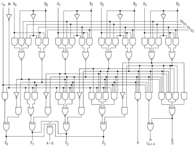
In 1967, Fairchild introduced the first ALU implemented as an integrated circuit, the Fairchild 3800, consisting of an eight-bit ALU with accumulator.[7] Other integrated-circuit ALUs soon emerged, including four-bit ALUs such as the Am2901 and 74181. These devices were typically «bit slice» capable, meaning they had «carry look ahead» signals that facilitated the use of multiple interconnected ALU chips to create an ALU with a wider word size. These devices quickly became popular and were widely used in bit-slice minicomputers.
Microprocessors began to appear in the early 1970s. Even though transistors had become smaller, there was often insufficient die space for a full-word-width ALU and, as a result, some early microprocessors employed a narrow ALU that required multiple cycles per machine language instruction. Examples of this includes the popular Zilog Z80, which performed eight-bit additions with a four-bit ALU.[8] Over time, transistor geometries shrank further, following Moore’s law, and it became feasible to build wider ALUs on microprocessors.
Modern integrated circuit (IC) transistors are orders of magnitude smaller than those of the early microprocessors, making it possible to fit highly complex ALUs on ICs. Today, many modern ALUs have wide word widths, and architectural enhancements such as barrel shifters and binary multipliers that allow them to perform, in a single clock cycle, operations that would have required multiple operations on earlier ALUs.
ALUs can be realized as mechanical, electro-mechanical or electronic circuits[9][failed verification] and, in recent years, research into biological ALUs has been carried out[10][11] (e.g., actin-based).[12]
See also[edit]
- Adder (electronics)
- Address generation unit (AGU)
- Load–store unit
- Binary multiplier
- Execution unit
References[edit]
- ^ a b A.P.Godse; D.A.Godse (2009). «3». Digital Logic Design. Technical Publications. pp. 9–3. ISBN 978-81-8431-738-1.
- ^ a b Leadership Education and Training (LET) 2: Programmed Text. Headquarters, Department of the Army. 2001. pp. 371–.
- ^ a b A.P.Godse; D.A.Godse (2009). «Appendix». Digital Logic Circuits. Technical Publications. pp. C–1. ISBN 978-81-8431-650-6.
- ^ «1. An Introduction to Computer Architecture — Designing Embedded Hardware, 2nd Edition [Book]». www.oreilly.com. Retrieved 2020-09-03.
- ^ Horowitz, Paul; Winfield Hill (1989). «14.1.1». The Art of Electronics (2nd ed.). Cambridge University Press. pp. 990–. ISBN 978-0-521-37095-0.
- ^ Philip Levis (November 8, 2004). «Jonathan von Neumann and EDVAC» (PDF). cs.berkeley.edu. pp. 1, 3. Archived from the original (PDF) on September 23, 2015. Retrieved January 20, 2015.
- ^ Lee Boysel (2007-10-12). «Making Your First Million (and other tips for aspiring entrepreneurs)». U. Mich. EECS Presentation / ECE Recordings. Archived from the original on 2012-11-15.
- ^
Ken Shirriff.
«The Z-80 has a 4-bit ALU. Here’s how it works.»
2013, righto.com - ^ Reif, John H. (2009), «Mechanical Computing: The Computational Complexity of Physical Devices», in Meyers, Robert A. (ed.), Encyclopedia of Complexity and Systems Science, New York, NY: Springer, pp. 5466–5482, doi:10.1007/978-0-387-30440-3_325, ISBN 978-0-387-30440-3, retrieved 2020-09-03
- ^ Lin, Chun-Liang; Kuo, Ting-Yu; Li, Wei-Xian (2018-08-14). «Synthesis of control unit for future biocomputer». Journal of Biological Engineering. 12 (1): 14. doi:10.1186/s13036-018-0109-4. ISSN 1754-1611. PMC 6092829. PMID 30127848.
- ^ Gerd Hg Moe-Behrens. «The biological microprocessor, or how to build a computer with biological parts».
- ^ Das, Biplab; Paul, Avijit Kumar; De, Debashis (2019-08-16). «An unconventional Arithmetic Logic Unit design and computing in Actin Quantum Cellular Automata». Microsystem Technologies. doi:10.1007/s00542-019-04590-1. ISSN 1432-1858. S2CID 202099203.
Further reading[edit]
- Hwang, Enoch (2006). Digital Logic and Microprocessor Design with VHDL. Thomson. ISBN 0-534-46593-5.
- Stallings, William (2006). Computer Organization & Architecture: Designing for Performance (7th ed.). Pearson Prentice Hall. ISBN 0-13-185644-8.
External links[edit]
Inside a computer, there is an Arithmetic Logic Unit (ALU), which is capable of performing logical operations (e.g. AND, OR, Ex-OR, Invert etc.) in addition to the arithmetic operations (e.g. Addition, Subtraction etc.). The control unit supplies the data required by the ALU from memory, or from input devices, and directs the ALU to perform a specific operation based on the instruction fetched from the memory. ALU is the “calculator” portion of the computer.
An arithmetic logic unit(ALU) is a major component of the central processing unit of the a computer system. It does all processes related to arithmetic and logic operations that need to be done on instruction words. In some microprocessor architectures, the ALU is divided into the arithmetic unit (AU) and the logic unit (LU).
An ALU can be designed by engineers to calculate many different operations. When the operations become more and more complex, then the ALU will also become more and more expensive and also takes up more space in the CPU and dissipates more heat. That is why engineers make the ALU powerful enough to ensure that the CPU is also powerful and fast, but not so complex as to become prohibitive in terms of cost and other disadvantages.
ALU is also known as an Integer Unit (IU). The arithmetic logic unit is that part of the CPU that handles all the calculations the CPU may need. Most of these operations are logical in nature. Depending on how the ALU is designed, it can make the CPU more powerful, but it also consumes more energy and creates more heat. Therefore, there must be a balance between how powerful and complex the ALU is and how expensive the whole unit becomes. This is why faster CPUs are more expensive, consume more power and dissipate more heat.
Different operation as carried out by ALU can be categorized as follows –
-
logical operations − These include operations like AND, OR, NOT, XOR, NOR, NAND, etc.
-
Bit-Shifting Operations − This pertains to shifting the positions of the bits by a certain number of places either towards the right or left, which is considered a multiplication or division operations.
-
Arithmetic operations − This refers to bit addition and subtraction. Although multiplication and division are sometimes used, these operations are more expensive to make. Multiplication and subtraction can also be done by repetitive additions and subtractions respectively.
Computer Architecture[edit | edit source]
2.1.1 Outline the architecture of the central processing unit (CPU) and the functions of the arithmetic logic unit (ALU) and the control unit (CU) and the registers within the CPU.
A major defining point in the history of computing was the realisation in 1944–1945 that data and instructions to manipulate data were logically the same and could be stored in the same place. The computer design built upon this principle, which became known as the von Neumann Architecture, is still the basis for computer today. Although the name honours John von Neumann, a brilliant mathematician who worked on the construction of the atomic bomb, the idea probably originated with J. Presper Echkert and John Mauchly, two other early pioneers who worked on the ENIAC at the Moore School at the University of Pennsylvania during the same time period.
Integrated circuits[edit | edit source]
Overview

An Integrated Circuit (or IC) is the central component of electronic devices or, as some say, “the heart and brains of most circuits” (SparkFun Learn). More commonly called a ‘chip’ or ‘microelectronic circuit’, an IC is a semiconducting wafer — usually made out of silicon (a semiconducting material) — on which tiny elements are placed to ensure the functioning of the device (such as resistors — which regulate the electric current — capacitors — which store energy — diodes — which signal current — and transistors — binary switch gates /see the What are Transistors? article). The capacity of such microchips fluctuates from thousands to millions of transistors, depending on the need of the machine.
Making-process: photolithography
ICs are made thanks to the repetition of a process called photolithography, a technique using light rays to transfer complex patterns onto patterned films of suitable material (often metal) placed onto the silicon wafer (a semiconducting material) ; to build transistors.
Fitting transistors onto an IC
The process is then repeated until all desired patterns are transferred onto the sample, which then becomes a transistor. See Moore’s Law graph (transistor page) to understand how the number of transistors which could be fitted in an IC evolved throughout the last decades.
ICs are electronic elements that are the equivalent of our DNA: they constitute the building bricks of the device, ensuring its basic functioning. Its role is thus key in the functioning of any unit, ensuring the simultaneous running of numerous actions (acting as an amplifier, an oscillator, a timer, a counter etc.) (Whatis.com, 2021).
Even if the first attempts of combining several electronic particles have been traced back to the 1920s, the first chip which could be compared to modern IC was made by Warner Jacobi, a German engineer who filed in 1949 a patent for his invention: a semiconductor amplifying device showing five transistors fitted on a three-stage amplifier arrangement (Wikipedia, 2022). However, most of the progress regarding ICs took place in the 60s, 70s and 80s, as engineers tried to overcome the Tyranny of Numbers problem (when millions of electronic parts were to be all assembled onto form one single chip, of which then hundreds of thousands were to be fitted onto a single computer thanks to the photolithographic process). In 2022, 63 years after Jacobi’s discovery, Apple managed to fit 114 billion transistors in its ARM-based dual-die M1 Ultra system, a chip using TSMC’s 5 nanometer (1 metre x 10-9) semiconductors (Wikipedia, 2022).
von Neumann Architecture[edit | edit source]
Another major characteristic of the von Neumann architecture is that the units that process information are separate from the units that store information. This characteristic leads to the following components of the von Neumann architecture.

- The memory unit that holds both data and instructions.
- The arithmetic/logic gate unit that is capable of performing arithmetic and logic operations on data.
- The input unit that moves data from the outside world into the computer.
- The output unit that moves results from inside the computer to the outside world.
- The control unit that acts as the stage unit to ensure that all the other components act in concert.
Memory[edit | edit source]
Memory is a collection of cells, each with a unique physical address. We use the generic word cell here rather than byte, because the number of bits in each addressable location, called the memory’s addressability, varies from one machine to another. Today, most computers are byte addressable.
To fully illustrate the concept of memory, take a computer with 4GB of RAM as an example. The memory consists of 4 × 230 bytes, which means each byte of the computer is uniquely addressable, and the addressability of the machine is 8 bits. The cells in memory are numbered consecutively beginning with 0. For example, if the addressability is 8, and there are 256 cells of memory, the cells would be addressed as follows:
| Address | Contents |
|---|---|
| 00000000 | 11100011 |
| 00000001 | 01010101 |
 |
|
| 11111100 | 00000000 |
| 11111101 | 11111111 |
| 11111110 | 10101010 |
| 11111111 | 00110011 |
What are the contents of address 11111110? The bit pattern stored at that location is 10101010. However, what the contents actually represents, be it instructions, value, sign, etc. will be discussed later. What is important, however, is to understand that the bit pattern is information and can be interpreted.
When referring to the bits in a byte or word, the bits are numbered from right to left beginning with zero. The bits in address 1111110 are numbered as follows:
| Bit Position | 7 | 6 | 5 | 4 | 3 | 2 | 1 | 0 |
|---|---|---|---|---|---|---|---|---|
| Contents | 1 | 0 | 1 | 0 | 1 | 0 | 1 | 0 |
Arithmetic/Logic Unit[edit | edit source]
The Arithmetic/Logic Unit (ALU) is capable of performing basic arithmetic operations such as adding, subtracting, multiplying, and dividing two numbers. This unit is also capable of performing logical operations such as AND, OR, and NOT. The ALU operates on words, a natural unit of data associated with a particular computer design. Historically, the word length of a computer has been the number of bits processed at once by the ALU. However, the current Intel line of processors has blurred this definition by defining the word length to be 16 bits. The processor can work on words (of 16 bits), double words (32 bits), and quadwords (64 bits). In the rest of this wiki, when referring to word, it will be of the historical nature aforementioned.
Most modern ALUs have a small number of special storage units called Registers. These registers contain one word and are used to store information that is needed again immediately. For example, in the calculation of 1 × (2 + 3). 2 is first added to 3 and the result is multiplied by 1. Rather than storing the result of adding 2 and 3 in memory and then retrieving it to multiply it by 1, the result is left in a register and the contents of the register is multiplied by 1. Access to registers is much faster than access to memory locations.
Input/Output Units[edit | edit source]
All of the computing power in the world would not be useful if one could not input values into the calculations from the outside or report to the outside the results of said calculations. Input and output units are the channels through which the computer communicates with the outside world.
An Input Unit is a device through which data and programs from the outside world are entered into the computer. The first input units interpreted holes punched on paper tape or cards. Modern-day input devices, however, include, but are not limited to; keyboards, mice, cameras (also known as, simply, webcams), and scanning devices.
An Output Unit is a device through which results stored in the computer memory are made available to the outside world. Examples include printers and screen monitors.
Peripheral devices refer to all hardware components that are connected / attached to the computer system but that are not part of the core computer architecture.
OS cannot interact with an exterior hardware device directly (there are always new ones coming out), therefore there is an intermediary called a device driver which is a type of software. Instead the device driver tells the OS what the peripheral device is and acts as a translator: the OS will send standard commands to the driver that will then translate them and drive them to the device.
A distinction can be made between input and output peripheral devices / units.
- Input devices: feed data that has been converted into electrical binary signals into the computer’s CPU.
- Example 1: Mouse. Data for a mouse would be the current mouse state (position of cursor, button state) which goes through the mouse driver that then informs the computer.
- Example 2: Microphone. Data is sound translated into electrical signals and goes through an audio driver.
Note that for a laptop for example these drivers and peripherals are integrated into the computer.
- Output devices: provides/displays data from the computer (outputs it).
- Example: Printer. Printers receive the data from the printer driver and output it on a page. Note how in some cases you have to manually download your printer’s driver as it is not integrated into the computer[1]
- Input/Output devices: some devices can do both: touchscreens, storage drives
| Classify the following into input and output devices: mouse, microphone, printer, keyboard, headphones, monitor, scanner. |
| Input: mouse, microphone, keyboard, scanner Output: printer, headphones, monitor |
[2][3]
Control Unit[edit | edit source]
The Control Unit is the organising force in the computer, for it is in charge of the Fetch-Execute Cycle. There are two special registers in the control unit. The Instruction Register (IR) contains the instruction that is being executed, and the Program Counter (PC) contains the address of the next instruction to be executed. Because the ALU and the control unit work so closely together they are often thought of as one unit called the Central Processing Unit (CPU).
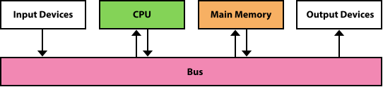
Above is a simplified view of the flow of information through the parts of a von Neumann machine. The parts are connected to one another by a collection of wires called a bus, through which data travels in the computer. Each bus carries three kinds of information; address, data, and control. An address is used to select the memory location or device to which data will go, or from which it will be taken. Data then flows over the bus between CPU, memory, and I/O Devices. The control information is used to manage the flow of addresses and data. For example, a control signal will typically be used to determine the direction in which the data is flowing either to or from the CPU. The Bus Width is the number of bits that it can transfer simultaneously. The wider the bus, the more address or data bits it can move at once.
2.1.3 Explain the use of cache memory.
Because memory accesses are very time consuming relative to the speed of the processor, many architectures provide Cache Memory. Cache memory is a small amount of fast-access memory into which copies of frequently used data are stored. Before a main memory access is made, the CPU checks whether the data is stored in the cache memory. Pipelining is another technique used to speed up the Fetch-Execute Cycle. This technique splits an instruction into smaller steps that can be overlapped.
In a personal computer, the component in a von Neumann machine reside physically a printed circuit board called the Motherboard. The motherboard also has connections for attaching other devices to the bus, such as a mouse, a keyboard, or additional storage devices.
So what does it mean to say that a machine is an n-bit processor? The variable n usually refers to the number of bits in the CPU general registers: Two n-bit numbers can be added with a single instruction. It also can refer to the width of the bus, which is the size of the addressable memory—but not always. In addition, n can refer to the width of the data bus—but not always.
The Fetch-Execute Cycle[edit | edit source]
2.1.4 Explain the machine instruction cycle.
Before looking at how a computer does what it does, let us look at what it can do. The definition of a computer outlines its capabilities; a computer is an electronic device that can store, retrieve, and process data. Therefore, all of the instructions that we give to the computer relate to storing, retrieving, and processing data.
The underlying principle of the von Neumann machine is that data and instructions are stored in memory and treated alike. This means that instructions and data are both addressable. Instructions are stored in contiguous memory locations; data to be manipulated are stored together in a different part of memory. To start the Fetch-Execute Cycle, first of all the data is loaded to the main memory by the operating system, the address of the first instruction is placed onto the program counter.

The process cycle includes four steps:
- Fetch the next instruction,
- Decode the instruction
- Get data if needed,
- Execute the instruction.
- Store result of execution and check for next instruction.
Fetch the Next Instruction[edit | edit source]
The PC increments one by one to point to the next instruction to be executed, so the control unit goes to the address in the memory address register which holds the address of the next instruction specified in the PC, takes it to the main memory through the address bus and returns it to the memory buffer register via the data bus. The MBR is a two way register that temporarily holds data fetched from the Memory(cache or RAM), makes a copy of the contents, and places the copy in the IR. At this point the IR contains the instruction to be executed. Before going to the next step in the cycle, the PC must be updated to hold the address of the next instruction to be executed when the current instruction has been completed. There after the instruction register is responsible for the instruction to be solved by the CU. the CU checks on the status of the instruction and then allows execution. Because the instructions are stored contiguously in memory, adding the number of bytes in the current instruction to the PC should put the address of the next instruction into the PC. Thus the control unit increments the PC. It is possible that the PC may be changed later by the instruction being executed.
In the case of an instruction that must get additional data from memory, the ALU sends an address to the memory bus, and the memory responds by returning the value at that location. In some computers, data retrieved from memory may immediately participate in an arithmetic or logical operation. Other computers simply save the data returned by the memory into a register for processing by a subsequent instruction. At the end of execution, any result from the instruction may be saved either in registers or in memory.
Decode the Instruction[edit | edit source]
To execute the instruction in the instruction register, the control unit has to determine what instruction it is. It might be an instruction to access data from an input device, to send data to an output device, or to perform some operation on a data value. At this phase, the instruction is decoded into control signals. That is, the logic of the circuitry in the CPU determines which operation is to be executed. This step shows why a computer can execute only instructions that are expressed in its own machine language. The instructions themselves are literally built into the circuit.
Get Data If Needed[edit | edit source]
The instruction to be executed may potentially require additional memory accesses to complete its task. For example, if the instruction says to add the contents of a memory location to a register, the control unit must get the contents of the memory location.
Execute the Instruction[edit | edit source]
Once an instruction has been decoded and any operands (data) fetched, the control unit is ready to execute the instruction. Execution involves sending signals to the arithmetic/logic unit to carry out the processing. In the case of adding a number to a register, the operand is sent to the ALU and added to the contents of the register.
When the execution is complete, the cycle begins again. If the last instruction was to add a value to the contents of a register, the next instruction probably says to store the results into a place in memory. However, the next instruction might be a control instruction—that is, an instruction that asks a question about the result of the last instruction and perhaps changes the contents of the program counter.
Hardware has changed dramatically in the last half-century, yet the von Neumann model remains the basis of most computers today. As Alan Perlis, a well-known computer scientist once said;
Sometimes I think the only universal in the computing field is the Fetch-Execute Cycle.
—Alan Perlis, 1981.
RAM and ROM[edit | edit source]
2.1.2 Describe primary memory.
RAM stands for Random-Access Memory. RAM is memory in which each cell (usually a byte) can be directly accessed. Inherent in the idea of being able to access each location is the ability to change the contents of each location. That is, storing something else into that place can change the bit pattern in each cell.
In addition to RAM, most computers contain a second kind of memory called ROM. ROM stands for Read-Only Memory. The contents in locations in ROM cannot be changed. Their contents are permanent and cannot be altered by a second operation. Placing the bit pattern in ROM is called burning. The bit pattern is burnt either at the time the ROM is manufactured or at the time the computer parts are assembled.
RAM and ROM are differentiated by a very basic property; RAM is volatile, and ROM is not. This means that RAM does not retain its bit configuration when the power is turned off, but ROM does. Because ROM is stable and cannot be changed, it is used to store the instructions that the computer needs to start itself. Frequently used software is also stored in ROM so that the system does not have to read the software each time the machine is turned on. Main memory usually contains some ROM along with the general-purpose RAM.
Secondary Storage Devices[edit | edit source]
2.1.5 Identify the need for persistent storage.
An input device is the means by which data and programs are entered into the computer and stored into memory. An output device is the means by which results are sent back to the user. Because most of main memory is volatile and limited, it is essential that there be other types of storage devices where programs and data can be stored when they are no longer being processed or when the machine is not turned on. These other types of storage devices (other than that of main memory) are called secondary or auxiliary storage devices. Because data must be read from them and written to them, each storage device is also an input and an output device.
Examples of secondary storage devices include;
- Magnetic Tape,
- Magnetic Disks,
- CDs and DVDs,
- Flash Drives,
- External Hardrives
Operating systems and application systems[edit | edit source]
2.1.6 Describe the main functions of an operating system.[edit | edit source]
As early as the end of the first generation of software development, there was a split between those programmers who wrote tools to help other programmers and those who used to solve problems. Modern software can be divided into two categories, system software and application software, reflecting this separation of goals. Application Software is written to address specific needs — to solve problems in the real world. Word processing programs, games, inventory control systems, automobile diagnostic programs, and missile guidance programs are all application software.
System Software manages a computer system at a more fundamental level. It provides the tools and an environment in which application software can be created and run. System software often interacts directly with the hardware and provides more functionality than the hardware does itself.
The Operating System of a computer is the core of its system software. An operating system manages computer resources, such as memory, and input/output devices, and provides an interface through which a human can interact with the computer. Other system software supports specific application goals, such as a library or graphics software that renders images on a display. The operating system allows an application program to interact with these other system resources.

The above diagram illustrates how an operating system interacts with many aspects of a computer system. The operating system manages hardware resources. It allows application software to access system resources, either directly or through other system software. It provides a direct user interface to the computer system.
2.1.7 Outline the use of a range of application software.[edit | edit source]
What are Computer Aided Design (CAD) softwares?
Computer Aided Design softwares are programs that can create digital designs on a computer. It is often used by architects, product designers, engineers, manufacturers, etc…
It allows users to create a design in 2D or 3D, visualize its construction, modify and optimize design processes, and view the final product.
Here’s a list of CAD softwares:
- AutoCAD: used for architectural, engineering, and industrial designs.
- SolidWorks: used for manufacturing and product design.
- Pro/Engineer (Creo): aerospace and automotive engineering.
- SketchUp: beginner friendly, good for architectural, interior, and landscape design
Example: Tesla
Tesla uses CAD to design their electric vehicles and their parts. They use these tools in order to create a complete 3D model of the car (interior and exterior). These models are mainly used to ensure that all the parts fit well together and function as predicted. They can also use these models to simulate the car’s performance in different situations, testing acceleration, charging time, wind resistance, fuel consumption, etc… This is also used to tweak the car’s aesthetic and appearance.
What are Web Browsers?[edit | edit source]
Examples of Web browsers
Google Chrome, Firefox, Safari, Opera, Internet Explorer
What is it?
A web browser is a general application software that allows access to websites. It is a software application that allows users to access and view web pages and other content on the internet. It retrieves information from web servers and displays it on the user’s device in a format that can be easily read and navigated.
Web browsers provide users with a graphical interface (GUI) that allows them to interact with web pages through menus, buttons, and other controls. They also support features such as bookmarks, history, and tabbed browsing, which allow users to easily navigate and manage their online activities.
How does it work?
The user, also called ‘client’, enters the URL of a website in the browser.
The browser then uses a world wide database called the DNS (Domain Name System) to match the website URL to the corresponding IP address. The IP address is a storage location which specifies where the website data is stored. The server is a computer hardware that stores data and provides functionality for other programs called ‘clients’.
The browser then makes a request to the server that has the IP address. The server then retracts the html (the source code) of the website which is itself either stored in the server or generated by the server.
This source code is received and read by the browser. Here’s a diagram of how it works:

Thus the purpose of a web browser is to bring information from a server to the client (through the request and response) allowing the client to view the information.
[4]
Memory, Process, and CPU Management[edit | edit source]
Recall that executing a program resides in main memory and its instructions are processed one after another in the fetch-decode-execute cycle. Multiprogramming is the technique of keeping multiple programs in main memory at the same time; these programs compete for access to the CPU so that they can do their work. All modern operating system employ multiprogramming to one degree or another. An operating system must therefore perform memory management to keep track of which programs are in memory and where in memory they reside.
Another key operating system concept is the idea of a process, which can be defined as a program in execution. A program is a static set of instructions. A process is a dynamic entity that represents the program while it is being executed. Through multiprogramming, a computer system might have many active processes at once. The operating system must manage these processes carefully. At any point in time a specific instruction may be the next to be executed. Intermediate values have been calculated. A process might be interrupted during its execution, so the operating system performs process management to carefully track the progress of a process and all of its intermediate states.
Related to the ideas of memory management and process management is the need for CPU scheduling, which determines which process in memory is executed by the CPU at any given point.
One must remember, however, that the OS itself is just a program that must be executed. Operating system processes must be managed and maintained in the main memory along with other system software and application programs. The OS executes on the same CPU as other programs, and it must take its turn among them.
The following sections (Single Contiguous Memory Management, Partition Memory Management, Paged Memory Management) are for interest purposes only. The Computer Science Guide clearly notes under 2.1.6 that «technical details are not needed. For example, memory management should be described but how this is handled in a multitasking environment is not expected.» Therefore, these sections serve the purpose of illustrating memory management techniques and can be summarised rather than utilised in an exam.
Single Contiguous Memory Management[edit | edit source]
Has only the operating system and one other program in memory at one time. This is the most basic type of memory management.
Partition Memory Management[edit | edit source]
The memory is broken up into different parts. Has the operating system and any number of programs running at the same time through these different partitions. The partitions have a base and a bound register.
Base register
- A register that holds the beginning address of the current partition (the one that is running)
Bounds register
- A register that holds the length of the current partition
Partition selection
First fit
- Allocate program to the first partition big enough to hold it
Best fit
- Allocated program to the smallest partition big enough to hold it
Worst fit
- Allocate program to the largest partition big enough to hold it
Paged Memory Management[edit | edit source]
A technique in which processes are divided into fixed-size pages and stored in memory frames when loaded.
Frame
- A fixed-size portion of main memory that holds a process page
Page
- A fixed-size portion of a process that is stored into a memory frame
Binary, decimal and hexadecimal representation of data[edit | edit source]
What is binary ?[edit | edit source]
The term binary refers to any encoding in which there are two possible values. In computer science they refer to the electronic values 0 and 1 (see figure below). Booleans values are binary. In computers we use binary instead of the decimal system as they offer a much simpler and efficient way to perform calculations through electronics than they would with a decimal system. This can be explored in the following sections regarding binary gates.

Interpretation of voltages to binary by the computer. Given that we are in a system where the max voltage is 5 Volts, then input current in an electrical wire is interpreted as a logical 0 by a transistor if the voltage is between 0 volts and 0.8 volts. On the other hand if the voltage is between 2 volts and 5 volts then the transistor interprets the input signal as a logical 1 (right diagram). It is important to note that there is a non-usable area of voltage that does not correspond to either a logical 0 or 1. This non-usable area is particularly useful since voltage always slightly fluctuates, having this grey zone allows us to better identify electrical signals (0 and 1) from each other. Similar voltage conversions from volts to binary digits also exist for output signals from transistors.¹
The base of a number system specifies the number of digits used in the system. The digits always begin with 0 and continue through one less than the base. For example, there are 2 digits in base 2: 0 and 1. There are 8 digits in base 8: 0 through to 7. There are 10 digits in base 10: 0 through 9. The base also determines what the positions of digits mean. When one adds 1 to the last digit in the number system, one has to carry the digit position to the left.
Positional notation[edit | edit source]
Numbers are written using positional notation. The rightmost digit represents its value multiplied by the base of the zeroth power. The digit to the left of that one represents its value multiplied by the base to the first power. The next digit represents its value multiplied by the base to the second power. The next digit represents its value multiplied by the base to the third power, and so on. One is usually familiar with positional notation even if they are not aware. One is instinctively inclined to utilise this method to calculate the number of ones in 943:
 |
 |
 |
 |
|
|
 |
|

|
|
 |
 |
|
 |
|
|
|
 |
|

|
|
 |
|
 |
|
|
|
 |
|
|

|
A more formal way of defining positional notation is to say that the value is represented as a polynomial in the base of a number system. But what is a polynomial? A polynomial is a sum of two or more algebraic terms, each of which consists of a constant multiplied by one or more variables raised to a non-negative integral power. When defining positional notation, the variable is the base of the number system. Thus 943 is represented as a polynomial as follows, with  acting as the base:

To express this idea formally, a number in the base- number system has
  digits, it is represented as follows, where
  represents the digit in the
  th position in the number:

Look complicated? Take a concrete example of 63578 in the base 10. Here is 5 (the number has exactly 5 digits), and is 10 (the base). The formula states that the fifth digit (the last digit on the left) is multiplied by the base to the fourth power; the fourth digit is multiplied by the base to the third power, and so on:

In the previous calculation, one assumed that the number base is 10. This is a logical assumption because the generic number system is base 10. However, there is no reason why the number 943 could not represent a value in base 13. In order to distinguish between these values, the general notation of  is utilised in order to represent a number
  in base . Therefore,
  is a number found in the base 10 system. In order to turn turn
  into
into  one simply uses the previous calculation:
|
|
 |
|
|
|
 |
|

|
|
|
|
|
 |
|
|
|
 |
|

|
|
|
|
 |
|
|
|
|
|
|

|
Therefore, 943 in base 13 is equal to 1576 in base 10, or  . One must keep in mind that these two numbers have an equivalent value. That is, both represent the same number of «things.» If one bag contains beans and a second bag contains beans, then both bags contain the exact same number of beans. The number systems just allow one to represent the value in various ways.
Note that in base 10, the rightmost digit is the «ones» position. In base 13, the rightmost digit is also the «ones» position. In fact, this is true for any base, because anything raised to the power of zero is one.
Why would anyone want to represent values in base 13? It is not done very often, granted, but it is sometimes helpful to understand how it works. For example, a computing technique called hashing takes numbers and scrambles them, and one way to scramble numbers is to interpret them in a different base.
Other bases, such as base 2 (binary), are particularly important in computer processing. It is also helpful to be familiar with number systems that are powers of 2, such as base 8 (octal), and base 16 (hexadecimal).
How is data stored in binary format ?[edit | edit source]
The following four questions are typically seen in Paper 1 Section A.
How many possible numbers can I store in a byte ?[edit | edit source]
A bit is the smallest unit of data that a computer can process and store. It can either store a 1 or a 0 and represents on/off, true/false, yes/no.
1 byte is a unit of data that consists of/stores 8 bits. 1 byte represents 28 distinct values.
- The biggest value a 1-byte number can be ( when all 8 bits are set to ) is: 11111111
- That represents: 27+26+25+24+23+22+21+20 = 255
How many possible numbers can I store in a an n-bit number ?
Since there are n possible bits that each can take two possible values (1 or 0), we can store  possible numbers in a n-bit number.
In a byte this means we can store 28 = 256 different numbers.
What is the biggest number I can get in a an n-bit number ?
Since there are n possible bits that each can take two possible values (1 or 0), the biggest number that we can get is 2n -1. Indeed the smallest number that we can get is a 0 hence the -1 in the formula.
In a byte this means the biggest number we can get is 28 -1 = 255, being 11111111, and the smallest number is 0 being 0000000.
How do I convert a base 2 (binary) number into a base 10 (decimal) number ?[edit | edit source]
To convert a binary number into decimal, we just need to sum all powers of 2 that have a 1 in the binary digit.
For example let’s take the binary number 1011. Following the previous rule of positional number we achieve the following table:
|
|
 |
|
|
|
 |
|
|
|
|
 |
|
 |
|
|
|
|
|
|
|
|
|
 |
|
|
|
 |
|
|
|
|
|
|

|
|
|
|
|
|
|

|
Now following the same logic, but just written differently, if we convert the following byte into decimal: 10011100
| 1 | 0 | 0 | 1 | 1 | 1 | 0 | 0 | |
|---|---|---|---|---|---|---|---|---|
| = | 27 | 26 | 25 | 24 | 23 | 22 | 21 | 20 |
| = | 128 | 64 | 32 | 16 | 8 | 4 | 2 | 1 |
| = | 128 | 16 | 8 | 4 |
We only add the columns where the binary digit is equal to 1. So 10011100 = 128 + 16 + 8 + 4 = 156
How do I convert a base 10 (decimal) number into a base 2 (binary) number ?[edit | edit source]
If we want to convert a decimal number to a binary number we will also use our previous conversion table.
For example let’s convert decimal number 56:
- First we look at the biggest binary power that can entirely fit in 56. This is 32 = 25. It is not 64 because 56 does not fit entirely into 64.
- Then we take the remainder of 56 — 32 = 24. We check which is the biggest binary power that can entirely fit into 24. This is 16 = 24.
- Then we take the remainder of 24 — 16 = 8. We check which is the biggest binary power that can entirely fit into 24. This is 8 = 23.
- Finally 8 — 8 = 0 so we have reached the end.
Now we mark the powers of two that we used for our calculus as a binary 1 and the other powers as 0. We get 00111000
| 27 | 26 | 25 | 24 | 23 | 22 | 21 | 20 | |
| = | 128 | 64 | 32 | 16 | 8 | 4 | 2 | 1 |
| = | 0 | 0 | 1 | 1 | 1 | 0 | 0 | 0 |
|---|
How are floats represented in binary ?[edit | edit source]
Section to go more in-depth on the content.
Floats are typically represented in 4 bytes. Out of these 32 bits: 1 bit is used for the sign of the number, 8 bits are used for the exponent and 23 bits are used for the floating point of the number. It is a way of storing numbers in scientific notation.

It is interesting to note that if we want to represent negative and positive numbers (whole numbers or decimal) we need to use one bit for storing the sign. If we only store positive numbers we don’t need to keep that sign bit.
Exercises — Binary representation of numbers[edit | edit source]
1. What is the decimal representation of 1001 ?
23 + 20 = 8 + 1 = 9
2. What is the decimal representation of 01000101 ?
26 + 22+ 20 = 64 + 4 + 1 = 69
3. What is the binary representation of 42 ?
42 — 32 = 10 with 32 = 24
10 — 8 = 2 with 8 = 23
2 — 2 = 0 with 2 = 21
Hence the binary representation: 00011010
4. What is the binary representation of 129 ?
129 — 128 = 1 with 128 = 27
1 — 1 = 0 with 1 = 20Hence the binary representation: 01000001
5. How many different integers can I represent in 2 bytes ?
2 bytes are 16 bits (2 x 8bits), hence 216 = 65536 different numbers can be represented in 2 bytes
6. What is the biggest number I can represent in 2 bytes ?
2 bytes are 16 bits (2 x 8bits), hence 216 -1 = 65535 is the biggest number that can be represented in 2 bytes.
It is also helpful to be familiar with number systems that are powers of 2, such as base 8 (octal), and base 16 (hexadecimal). Recall that base 10 has ten digits (0−9), base 2 has two digits (0−1), and base 8 has eight digits (0−7). Therefore, the number 943 could not represent a value in any base less than 10, because the digit 9 does not exist in those bases. It is, however, a valid number in base 10 or any base higher than that. Likewise, the number 2074 is a valid number in base 8 or higher, but it simply does not exist (because it uses the digit 7) in any base lower than that.
What are the digits in bases higher than 10? One needs to assign symbols to represent the digits that correspond to the decimal values 10 and beyond. In bases higher than 10, one generally looks towards letters as digits. The letter A, consequently, will represent the number 10, B to represent 11, C to represent 12, and so forth. All digits are written in the following conversion table.
What is Hexadecimal ?[edit | edit source]
| decimal | hexadecimal | binary |
|---|---|---|
| 0 | 0 | 0000 |
| 1 | 1 | 0001 |
| 2 | 2 | 0010 |
| 3 | 3 | 0011 |
| 4 | 4 | 0100 |
| 5 | 5 | 0101 |
| 6 | 6 | 0110 |
| 7 | 7 | 0111 |
| 8 | 8 | 1000 |
| 9 | 9 | 1001 |
| 10 | A | 1010 |
| 11 | B | 1011 |
| 12 | C | 1100 |
| 13 | D | 1101 |
| 14 | E | 1110 |
| 15 | F | 1111 |
Hexadecimal is a numbering system that uses 16 possible digits. Its primary attraction is its ability to represent very high numbers with fewer digits that in binary or in the decimal system.
How do I convert a decimal number to a hexadecimal number ?[edit | edit source]
The method is following:
- Apply a floor division to the decimal number by 16. Write down the remainder.
- Continue applying floor division by 16 to the previous result of the floor division until you reach 0. Keep writing down the remainders.
- Convert the remainders, from last one to first one, to hexadecimal.
- You have your hexadecimal number !
For example if we want to convert the decimal number 2545 to hexadecimal:
- We apply floor division: 2545 // 16 = 159, The remainder of that division is 2545 % 16 = 1
- We apply floor division to our previous result: 159 // 16 = 9, The remainder of that division is 159 % 16 = 15
- We apply floor division to our previous result: 9 // 16 = 0, The remainder of that division is 9 % 16 = 9.
- We reached 0 so we stop dividing.
- We convert our remainders: 9 → 9, 15 → F, 1 → 1
- So our hexadecimal number is: 9F1
How do I convert a hexadecimal number to a decimal number ?[edit | edit source]
This conversion is a bit simpler as we can use the positional notation to convert our number. Indeed we just need to multiply each hexadecimal digit by its corresponding power of 16.
For example if we want to convert the hexadecimal number ABC to decimal we can do the following:
 |
|
 |
|
|
|
 |
|

|
|
|
 |
|
 |
|
|
|
 |
|

|
|
 |
|
 |
|
 |
|
|
|
12 |

|
How do I convert a binary number to a hexadecimal number ?[edit | edit source]
To easily convert a binary number to a hexadecimal number you just need to split your binary number in groups of 4 bits. If the length of your binary number is not an exact multiplication of 4, just add 0s to the left side of your binary number until you reach a multiple of 4.
Then convert your groups of 4 bits to their corresponding hexadecimal characters and you will have your hexadecimal number !
For example if we want to convert the binary number: 1011111011
- Our number has 10 bits so we add two 0s to the left side: 001011111011
- We divide our number in groups of 4 bits: 0010 1111 1011
- We convert the binary number to hexadecimal numbers: 0010 → 2, 1111 → F, 1011 → B
- Our hexadecimal number is 2FB
What is Octal ?[edit | edit source]
Not needed for the exams
Octal is a numbering system in base 8, meaning only digits from 0 to 7 exist in this notation.
For example, one can calculate the decimal equivalent of 754 in octal (base  − simply put, finding
  . As before, it is the case of expanding the number in its polynomial form and adding up the numbers:
 |
|
 |
|
|
|
 |
|

|
|
|
 |
|
 |
|
|
|
|
|
|
|
|
|
 |
|
|
|
|
|
|

|
Simple logic gates[edit | edit source]
Use BOOLR to practice using logic gates.
2.1.11 Define the Boolean operators; AND, OR, NOT, NAND, NOR, and XOR.
2.1.12 Construct truth tables using the above operators.
The gates in a computer are sometimes referred to as logic gates because they each perform just one logical function. That is, each gate accepts one or more input values and produces a single output value. Because one is dealing with binary information, each input and output is either 0, corresponding a low-voltage signal, or 1, corresponding to a high-voltage signal. The type of gate and the input values determine the output value.
Gate Definitions[edit | edit source]
NOT Gate[edit | edit source]
| Boolean Expression | Logic Diagram Symbol | Truth Table | ||||||
|---|---|---|---|---|---|---|---|---|
X = A' |
A X |
|
A NOT gate accepts one input value and produces one output value. The table to the right illustrates a NOT gate in three ways; as a Boolean expression, as its logical diagram symbol, and using a truth table. In each representation, the variable A represents the input signal, which is either 0 or 1. The variable X represents the output signal, whose value (0 or 1) is determined by the value of A.
By definition, if the input value for a NOT gate is 0, the output is 1; if the input value is 1, the output is 0. A NOT gate is sometimes referred to as an inverter because it inverts the input value.
In Boolean expressions, the NOT operation is represented by the ' mark after the value begin negated. Sometimes this operation is shown as a horizontal bar over the value begin negated. In the Boolean expression in the table, X is assigned to the value determined by applying a NOT operation to input value A. In such an assignment statement, the variable on the left of the equal sign takes on the value of the expression on the right-hand side.
The logical diagram symbol for a NOT gate is a triangle with a small circle (called an inversion bubble) on the end. The input and output are shown as lines flowing into and out of the gate. Sometimes these lines are labeled, though not always.
The truth table shows all possible input values for a NOT gate as well as the corresponding output values. Because there is only one input signal to a NOT gate, and that signal can only be 0 or 1, there are only two possibilities for the column labelled A in the truth table. The column labelled X shows the output of the gate, which is the inverse of the input. Note that of the three representations, only the truth table actually defines the behaviour of the gate for all situations.
These three notations are just different ways of representing the same thing, for example, the result of the Boolean expression 0' is always 1, and the result of the Boolean expression 1' is always 0. This behaviour is consistent with the values shown in the truth table.
AND Gate[edit | edit source]
| Boolean Expression | Logic Diagram Symbol | Truth Table | |||||||||||||||||||
|---|---|---|---|---|---|---|---|---|---|---|---|---|---|---|---|---|---|---|---|---|---|
X = A • B
|
|
|

Unlike the NOT gate, which accepts one input signal, an AND gate accepts two input signals. The values of both input signals determine what the output signal will be. If the two input values for an AND gate are both 1, the output is 1; otherwise, the output is 0.
The AND operation in Boolean algebra is expressed using a single dot (•) or, in some cases, an asterisk (*). Often the operator itself is assumed, for example A•B is often written as AB.
Because there are two inputs and two possible values for each input, four possible combinations of 1 and 0 can be provided as input to an AND gate. Therefore, four situations can occur when the AND operator is used in a Boolean expression.
Likewise, the truth table showing the behaviour of the AND gate has four rows, showing all four possible input combinations.
OR Gate[edit | edit source]
| Boolean Expression | Logic Diagram Symbol | Truth Table | |||||||||||||||||||
|---|---|---|---|---|---|---|---|---|---|---|---|---|---|---|---|---|---|---|---|---|---|
X = A + B
|
|
|

Like the AND gate, there are two inputs to an OR gate. If the two input values are both 0, the output value is 0; otherwise, the input is 1.
The Boolean algebra OR operation is expressed using a plus sign (+). The OR gate has two inputs, each of which can be one of two values, so as with an AND gate there are four input combinations and therefore four rows in the truth table.
XOR Gate[edit | edit source]
| Boolean Expression | Logic Diagram Symbol | Truth Table | |||||||||||||||||||
|---|---|---|---|---|---|---|---|---|---|---|---|---|---|---|---|---|---|---|---|---|---|
X = A ⊕ B
|
|
|

The XOR, or exclusive OR, gate is illustrated to the right. An XOR gate produces 0 if its two inputs are the same, and 1 otherwise. Note the difference between the XOR gate and the OR gate; they differ only in one input situation. When both input signals are 1, the OR gate produces a 1 and the XOR produces a 0.
Sometimes the regular OR gate is referred to as the inclusive OR, because it produces a 1 if either or both of its inputs is a 1. The XOR produces a 1 only if its inputs are mixed, one 1 and one 0. Think of XOR gates as saying, «When I say or, I mean one or the other, no both.»
The Boolean algebra symbol ⊕ is sometimes used to express the XOR operation. However, the XOR operation can also be expressed using the other operators; we leave that as an exercise.
Note that the logic diagram symbol for the XOR gate is just like the symbol for an OR gate except that it has an extra curved line connecting its input signals.
NAND and NOR Gates[edit | edit source]
| NAND Gate | |||||||||||||||||||||
|---|---|---|---|---|---|---|---|---|---|---|---|---|---|---|---|---|---|---|---|---|---|
| Boolean Expression | Logic Diagram Symbol | Truth Table | |||||||||||||||||||
X = (A • B)'
|
|
|
|||||||||||||||||||
| NOR Gate | |||||||||||||||||||||
| Boolean Expression | Logic Diagram Symbol | Truth Table | |||||||||||||||||||
X = (A + B)'X = A - B
|
|
|


The NAND and the NOR gate accept two input values. The NAND and NOR gates are essentially the opposite of the AND and OR gates, respectively. That is, the output of a NAND gate is the same as if one took the output of an AND gate and put it through an inverter (a NOT gate).
There are typically no specific symbols used to express the NAND and NOR gates operations in Boolean algebra. Instead, one should rely on their definitions to express the concepts. That is, the Boolean algebra expression for NAND is the negation of the AND operation. Likewise, the Boolean algebra expression for NOR is the negation of an OR operation.
The logic diagram symbols for the NAND and NOR are the same as those for the AND and OR except that the NAND and NOR symbols have the inversion bubble (to indicate the negation). Compare the output columns for the truth tables for the AND and NAND. They are the opposite, row by row. The same is true for OR and NOR gates.
Review of Gate Processing[edit | edit source]
Six specific types of gates have been observed. It may seem to be a difficult task to keep them straight and remember how they all work. Well, that probably depends on how one thinks about it. One should not be encouraged to try and memorise truth tables. The processing of these gates can be described briefly in general terms. If one thinks of them that way, one can produce the appropriate truth table any time needed.
Some of these descriptions are in terms of what input values cause the gate to produce as 1 as a n output; in any other case, it produces a 0:
- A NOT gate inverts its single input value,
- An AND gate produces 1 if both input values are 1,
- An OR gate produces 1 if one or the other or both input values are 1,
- An XOR gate produces 1 if one or the other (but not both) input values are 1,
- A NAND gate produces the opposite results of an AND gate, and
- A NOR gate produces the opposite results of an OR gate.
How to Construct a Truth Table[5][edit | edit source]

A truth table is a visual representation of the various inputs of a circuit and the outputs that are associated with each combination of inputs. To create a truth table, draw a table sequentially with one column for each input and one or more columns for the output. The image to the right represents a truth table to Q= A NOR B. In the first row, write the name of your inputs and output in order as seen in the image. Then, on the second column, set both inputs to 0 and determine the output depending on your gate. Then, for each new row, increment the inputs by 1 and determine the output based on those inputs. Depending on the inputs and on the boolean gate, the output will change in each row. In the last column, put the output of the function for each combination of inputs.
Constructing Gates[edit | edit source]
2.1.13 Construct a logic diagram using AND, OR, NOT, NAND, NOR, and XOR.
Combinational Circuits[edit | edit source]
A combinational circuit consists of logic gates whose outputs are determined at any time from the present combination of inputs irrespective of previous inputs.It consists of input variables, logic gates and output variables. The logic gate accept signals from inputs and generate signals at the outputs.Some of the examples of combinational circuits are binary adder, decimal adder,decoder,multiplexer,half adder, half subtractor etc.
Arithmetic circuits[edit | edit source]
Adders[edit | edit source]
Half adder[edit | edit source]

A logic circuit for the addition of two one-bit numbers is called a half adder. There must be two bits output: the sum of the addition (either a 1 or 0) and whether or not you carry a bit. The carry comes from the addition of 1 + 1, which equals 10 (binary 2). The addition process is reproduced in this truth table.
| A | B | Sum | Carry |
|---|---|---|---|
| 0 | 1 | 1 | 0 |
| 1 | 0 | 1 | 0 |
| 1 | 1 | 0 | 1 |
Multiplexers[edit | edit source]
BOOLEAN EXPRESSION:
D0 = X’Y’  ,  D1 = X’Y
D2 = XY’  ,  D3 = XY
- ↑ «Download printer drivers in Windows — Microsoft Support». support.microsoft.com. Retrieved 2023-04-05.
- ↑ «PC mouse info». courses.cs.washington.edu. Retrieved 2023-04-05.
- ↑ «Peripheral device | Definition & Examples | Britannica». www.britannica.com. Retrieved 2023-04-05.
- ↑ How The Web Works — The Big Picture, retrieved 2023-04-05
- ↑ Weisman, Jeremy (2022). Computer Science 2nd Int 2022. p. 1.
Introduction
Arithmetic and logic unit (arithmetic and logic unit) is a combinational logic circuit that can realize multiple sets of arithmetic operations and logic operations, or ALU for short.
Arithmetic&logical Unit is the execution unit of the central processing unit (CPU), which is the core component of all central processing units, and is composed of «And Gate» (AND Gate) and «Or Gate» (OR Gate) arithmetic logic Unit, the main function is to perform two-bit arithmetic operations, such as addition, subtraction and multiplication (excluding integer division). Basically, in all modern CPU architectures, binary is represented in the form of complement.
Development
Arithmetic logic unit (ALU) is a structure that performs integer operations. At this stage, it is implemented with a circuit, which is used in computer chips.
In a computer, an arithmetic logic unit (ALU) is a digital circuit that specifically performs arithmetic and logical operations. ALU is the most important part of the computer’s central processor. Even the smallest microprocessor contains ALU as a counting function. Modern CPUs and GPU processors already contain powerful and complex ALUs; a single component may also contain ALUs.
In 1945, the mathematician von Neumann proposed the concept of ALU in a report introducing the basic structure of a new computer called EDVAC.

Early development
In 1946, von Neumann worked with colleagues to design a computer for the Princeton Advanced Learning Institute (IAS). Then the IAS computer became the prototype of the later computer. In the paper, von Neumann mentions the parts he believes are needed in computers, including ALU. Von Neumann wrote that ALU is an essential part of a computer because it has been determined that the computer must complete basic mathematical operations, including addition, subtraction, multiplication and division. So he believed that «(the computer) should contain components that specifically perform such operations.
Digital system
The ALU must use the same format for digital processing as the rest of the digital circuit. For modern processors, the values are always expressed in two’s complement. Earlier computers used many digital systems, including inverse codes, symbolic numeric codes, and even decimal codes, each using ten tubes. The ALUs corresponding to each of the above digital systems have different designs, and this also affects the current preference for two’s complement, because two’s complement can simplify ALU addition and subtraction operations. A simple 2-bit ALU that can perform NAND AND AND addition.
Feasibility Analysis
Most computer instructions are executed by ALU. ALU takes data from the register. The data is processed and the operation result is stored in the ALU output register. Other components are responsible for transferring data between registers and memory. The control unit controls the ALU and tells the ALU what operation to perform through the control circuit.
Simple operation
Most ALUs can complete the following operations:
Integer arithmetic operations (addition and subtraction, sometimes including multiplication and division, but the cost is higher)
Bit logic operation (AND, OR, NOT, XOR)
Shift operation (shift or float a word to the left or right by a specific bit without unsigned extension), the shift can be considered as multiplying by 2 or dividing by 2.
Complex operations
Engineers can design an ALU that can perform any operation, no matter how complex the operation is; the problem is that the more complex the operation, the higher the cost of the ALU, the more space it takes in the processor, and the more power it consumes. As a result, engineers often calculate a compromise solution and provide the processor (or other circuit) with an ALU that can make it operate at high speed, but at the same time avoid the ALU design being too complicated and expensive. Imagine that you need to calculate the square root of a number. The digital engineer will evaluate the following options to accomplish this:
Design an extremely complex ALU, which can complete the square root operation of any number in one step. This is called single clock calculation.
Design a very complex ALU, which can complete the square root operation of a number in several steps. However, there is a trick here, the intermediate result goes through a series of circuits, like a production line in a factory. This even allows the ALU to accept new numbers before completing the previous operation. This allows the ALU to produce numbers at the same speed as a single clock pulse, although the results output from the ALU have an initial delay. This is called a calculation pipeline.
Design a complex ALU that can calculate the square root of a number in several steps. This is called interactive computing and often relies on complex control units with embedded microcode.
Design a simple ALU in the processor, remove an expensive processor dedicated to this operation, and choose one of the above three options. This is called a coprocessor.
told programmers that there were no coprocessors and emulated devices, so they had to write their own algorithms to calculate the square root in software. This is done by the software library.
Simulate the coprocessor, that is to say, whenever a program wants to calculate the square root, let the processor check whether there is a coprocessor. If there is, use it to calculate, if not, interrupt the program process and call the operating system to complete the square root calculation through the software algorithm. This is called software emulation.
The options given above are ranked from fastest and most expensive to slowest and most economical. So, even the simplest computer can calculate the most complex formulas, but the simplest computer often takes a lot of time and can be completed in several steps. Powerful processors such as the Intel Core and AMD64 series use option 1 for some simple operations, option 2 for the most common complex operations, and option 3 for extremely complex operations. This is premised on the ability to construct very complex ALUs in the processor.
Input and output
The input of the ALU is the data to be operated (called operands) and the instruction code from the control unit, which is used to indicate which operation to perform. Its output is the operation result. In many designs, the ALU also receives or sends input or output condition codes to (or from) the status register. These codes are used to indicate some conditions, such as carry or borrow, overflow, and division by zero.
ALU and FPU
The floating-point unit also performs arithmetic operations on two values, but this operation has been represented by floating-point numbers, which is much more complicated than the two’s complement representation method generally used in ALU. In order to complete such operations, multiple complex circuits are embedded in the FPU, including some internal ALUs. Engineers generally think that ALU is a circuit that handles arithmetic operations of integer types (such as complement and BCD), while circuits that calculate more complex formats (such as floating-point and complex numbers) have a more matching title.
Features
ALU is used to perform arithmetic and logic operations in the computer instruction set;
In some processors, the ALU is divided into two parts, the arithmetic unit (AU) and the logic unit (LU). Some processors contain more than one AU, for example, one for fixed-point operations and another for floating-point operations. (In personal computers, floating-point operations are sometimes performed by floating-point units called digital coprocessors).
Generally speaking, ALU has the right to read and write directly to the processor controller, memory and input and output devices. Input and output are performed via the bus. The input instruction contains an instruction word, sometimes called a machine instruction word, which includes an operation code, a single or multiple operands, and sometimes a format code; the operation code indicates what operation the ALU machine is to perform, and in this operation How many operands. For example, two operands can be compared or added. The format code can be combined with the opcode to tell whether this is a fixed-point or floating-point instruction; the output includes the result stored in the storage register and the setting that shows whether the operation was successful. If the operation fails, there will be a corresponding status display in the machine status word.
Generally, the storage locations of input operands, operands, accumulated sums, and conversion results are all in the ALU. In the arithmetic unit, the multiplication and division operations are obtained through a series of addition and subtraction operations. There are multiple ways to represent negative numbers in machine code.
In the logical unit, one of 16 possible logical operations is executed at a time.
The design of the ALU is a key part of the processor design. Continue to study how to increase the processing speed of instructions.
Logical unit
A logic unit (LU) is a network port that enters the IBM System Network Architecture (SNA), through which users can access network resources, or one programmer can communicate with another programmer.
Computer Architecture
Joe Grimes, in Encyclopedia of Physical Science and Technology (Third Edition), 2003
VI.B.1 ALU
The ALU is a combinational circuit, and is that part of the processor that performs arithmetic, logic, and other necessary related operations. Sometimes there is a separate component, shifter, which is used to perform the shift operations on data items. The abstraction 2 programmer usually considers the shifter activities to be a part of the ALU. The Abacus, Blaise Pascal machine, and other ancestors of the computer were really just ALUs, and for the most part the other components of modern computer systems are merely there to hold data for or transfer it to the ALU. Thus, the ALU could be considered the center of the computer system. However, it does not determine its own activities. Abstraction 1 or 2 instructions determine its activity via the control. The ALU will be actively involved in steps 2, 3, and 5 of the instruction cycle of Example VIB and may be involved in other steps.
Read full chapter
URL:
https://www.sciencedirect.com/science/article/pii/B0122274105001319
Microarchitecture
Sarah L. Harris, David Harris, in Digital Design and Computer Architecture, 2022
7.3.3 Single-Cycle Control
The single-cycle processor’s control unit computes the control signals based on op, funct3, and funct7. For the RV32I instruction set, only bit 5 of funct7 is used, so we just need to consider op (Instr6:0), funct3 (Instr14:12), and funct75 (Instr30). Figure 7.12 shows the entire single-cycle processor with the control unit attached to the datapath.

Figure 7.12. Complete single-cycle processor
Figure 7.13 hierarchically decomposes the control unit, which is also referred to as the controller or the decoder, because it decodes what the instruction should do. We partition it into two major parts: the Main Decoder, which produces most of the control signals, and the ALU Decoder, which determines what operation the ALU performs.

Figure 7.13. Single-cycle processor control unit
Table 7.2 shows the control signals that the Main Decoder produces, as we determined while designing the datapath. The Main Decoder determines the instruction type from the opcode and then produces the appropriate control signals for the datapath. The Main Decoder generates most of the control signals for the datapath. It also produces internal signals Branch and ALUOp, signals used within the controller. The logic for the Main Decoder can be developed from the truth table using your favorite techniques for combinational logic design.
Table 7.2. Main Decoder truth table
| Instruction | Op | RegWrite | ImmSrc | ALUSrc | MemWrite | ResultSrc | Branch | ALUOp |
|---|---|---|---|---|---|---|---|---|
| lw | 0000011 | 1 | 00 | 1 | 0 | 1 | 0 | 00 |
| sw | 0100011 | 0 | 01 | 1 | 1 | x | 0 | 00 |
| R-type | 0110011 | 1 | xx | 0 | 0 | 0 | 0 | 10 |
| beq | 1100011 | 0 | 10 | 0 | 0 | x | 1 | 01 |
The ALU Decoder produces ALUControl based on ALUOp and funct3. In the case of the sub and add instructions, the ALU Decoder also uses funct75 and op5 to determine ALUControl, as given in in Table 7.3. ALUOp of 00 indicates add (e.g., to find the address for loads or stores). ALUOp of 01 indicates subtract (e.g., to compare two numbers for branches). ALUOp of 10 indicates an R-type ALU instruction where the ALU Decoder must look at the funct3 field (and sometimes also the op5 and funct75 bits) to determine which ALU operation to perform (e.g., add, sub, and, or, slt).
Table 7.3. ALU Decoder truth table
| ALUOp | funct3 | {op5, funct75} | ALUControl | Instruction |
|---|---|---|---|---|
| 00 | x | x | 000 (add) | lw, sw |
| 01 | x | x | 001 (subtract) | beq |
| 10 | 000 | 00, 01, 10 | 000 (add) | add |
| 000 | 11 | 001 (subtract) | sub | |
| 010 | x | 101 (set less than) | slt | |
| 110 | x | 011 (or) | or | |
| 111 | x | 010 (and) | and |
According to Table B.1 in the inside covers of the book, add, sub, and addi all have funct3 = 000. add has funct7 = 0000000 while sub has funct7 = 0100000, so funct75 is sufficient to distinguish these two. But we will soon consider supporting addi, which doesn’t have a funct7 field but has an op of 0010011. With a bit of thought, we can see that an ALU instruction with funct3 = 000 is sub if op5 and funct75 are both 1, or add or addi otherwise.
Example 7.1
Single-cycle Processor Operation
Determine the values of the control signals and the portions of the datapath that are used when executing an and instruction.
Solution
Figure 7.14 illustrates the control signals and flow of data during execution of an and instruction. The PC points to the memory location holding the instruction; the instruction memory outputs this instruction. The main flow of data through the register file and ALU is represented with a heavy blue line. The register file reads the two source operands specified by Instr. SrcB should come from the second port of the register file (not ImmExt), so ALUSrc must be 0. The ALU performs a bitwise AND operation, so ALUControl must be 010. The result comes from the ALU, so ResultSrc is 0, and the result is written to the register file, so RegWrite is 1. The instruction does not write memory, so MemWrite is 0.

Figure 7.14. Control signals and data flow while executing an and instruction
The updating of PC with PCPlus4 is shown by a heavy gray line. PCSrc is 0 to select the incremented PC. Note that data does flow through the nonhighlighted paths, but the value of that data is disregarded. For example, the immediate is extended and a value is read from memory, but these values do not influence the next state of the system.
Read full chapter
URL:
https://www.sciencedirect.com/science/article/pii/B9780128200643000076
Technique to Manage Software Safety
Jean-Louis Boulanger, in Certifiable Software Applications 1, 2016
6.5 Glossary
- ALU
-
Arithmetic Logic Unit
- CENELEC
-
6Comité Européen de Normalisation Electrotechnique (European Committee for Electrotechnical Standardization)
- CRC
-
Cyclic Redundancy Check
- E/E/PES
-
Electric/Electronic/Programmable Electronic systems
- EEPROM
-
Electrically Erasable Programmable Read-Only Memory
- EMC
-
Electromagnetic Compatibility
- EPROM
-
Erasable Programmable Read-Only Memory
- FPU
-
Floating Point Unit
- IEC
-
7International Electrotechnical Commission
- ISO
-
8International Organization for Standardization
- OS
-
Operating System
- PLC
-
Programmable Logic Controller
- PROM
-
Programmable Read-Only Memory
- QA
-
Quality Assurance
- RAM
-
Random Access Memory
- RAMS
-
Reliability, Availability, Maintainability and Safety
- RAMSS
-
Reliability, Availability, Maintainability, Safety and Security
- ROM
-
Read-Only Memory
- SA
-
Safety Assurance
- SIL
-
Safety Integrity Level
- VRAM
-
Video RAM
Read full chapter
URL:
https://www.sciencedirect.com/science/article/pii/B9781785481178500064
Domain 3
Eric Conrad, … Joshua Feldman, in Eleventh Hour CISSP® (Third Edition), 2017
The CPU
The central processing unit (CPU) is the brains of the computer, capable of controlling and performing mathematical calculations. Ultimately, everything a computer does is mathematical: adding numbers, which can be extended to subtraction, multiplication, division, etc.; performing logical operations; accessing memory locations by address; etc. CPUs are rated by the number of clock cycles per second. A 4-GHz CPU has four billion clock cycles per second.
Arithmetic logic unit and control unit
The arithmetic logic unit (ALU) performs mathematical calculations; it is the part that computes. The ALU is fed instructions by the control unit, which acts as a traffic cop, sending instructions to the ALU.
Fetch and execute
CPUs fetch machine language instructions (such as “add 1 + 1”) and execute them (add the numbers, for answer of “2”). The “fetch and execute” (also called the fetch-decode-execute cycle or FDX) process actually takes four steps:
- 1.
-
Fetch Instruction 1
- 2.
-
Decode Instruction 1
- 3.
-
Execute Instruction 1
- 4.
-
Write (save) Result 1
These four steps take one clock cycle to complete.
Pipelining
Pipelining combines multiple CPU steps into one process, allowing simultaneous FDX and write steps for different instructions. Each part is called a pipeline stage; the pipeline depth is the number of simultaneous stages that may be completed at once.
Given our previous fetch-and-execute example of adding 1 + 1, a CPU without pipelining would have to wait an entire cycle before performing another computation. A four-stage pipeline can combine the stages of four other instructions:
- 1.
-
Fetch Instruction 1
- 2.
-
Fetch Instruction 2, Decode Instruction 1
- 3.
-
Fetch Instruction 3, Decode Instruction 2, Execute Instruction 1
- 4.
-
Fetch Instruction 4, Decode Instruction 3, Execute Instruction 2, Write (save) result 1
- 5.
-
Fetch Instruction 5, Decode Instruction 4, Execute Instruction 3, Write (save) result 2, etc.
Pipelining is like an automobile assembly line; instead of building one car at a time, from start to finish, lots of cars enter the assembly pipeline, and discrete phases (like installing tires) occur on one car after another. This increases the throughput.
Interrupts
An interrupt indicates that an asynchronous event has occurred. A CPU interrupt is a form of hardware interrupt that causes the CPU to stop processing its current task, save the state, and begin processing a new request. When the new task is complete, the CPU will complete the prior task.
Processes and threads
A process is an executable program and its associated data loaded and running in memory. A heavyweight process (HWP) is also called a task. A parent process may spawn additional child processes called threads. A thread is a lightweight process (LWP). Threads are able to share memory, resulting in lower overhead compared to heavy weight processes.
Multitasking and multiprocessing
Applications run as processes in memory, comprised of executable code and data. Multitasking allows multiple tasks (heavyweight processes) to run simultaneously on one CPU. Older and simpler operating systems, such as MS-DOS, are non-multitasking, in that they run one process at a time. Most modern operating systems, such as Linux, Windows 10, and OS X support multitasking.
Multiprocessing has a fundamental difference from multitasking: it runs multiple processes on multiple CPUs. Two types of multiprocessing are symmetric multiprocessing (SMP) and asymmetric multiprocessing (AMP; some sources use ASMP). SMP systems have one operating system to manage all CPUs. AMP systems have one operating system image per CPU, essentially acting as independent systems.
CISC and RISC
CISC (complex instruction set computer) and RISC (reduced instruction set computer) are two forms of CPU design. CISC uses a large set of complex machine language instructions, while RISC uses a reduced set of simpler instructions. x86 CPUs, among many others, are CISC; ARM (used in many cell phones and PDAs), PowerPC, Sparc, and others are RISC.
Read full chapter
URL:
https://www.sciencedirect.com/science/article/pii/B9780128112489000036
Domain 6
Eric Conrad, … Joshua Feldman, in CISSP Study Guide (Second Edition), 2012
The CPU
The central processing unit (CPU) is the brains of the computer, capable of controlling and performing mathematical calculations. Ultimately, everything a computer does is mathematical: adding numbers (which can be extended to subtraction, multiplication, division, etc), performing logical operations, accessing memory locations by address, etc. CPUs are rated by the number of clock cycles per second. A 2.4-GHz Pentium® 4 CPU has 2.4 billion clock cycles per second.
Arithmetic logic unit and control unit
The arithmetic logic unit (ALU) performs mathematical calculations—it computes. It is fed instructions by the control unit, which acts as a traffic cop, sending instructions to the ALU.
Fetch and execute
CPUs fetch machine language instructions (such as “add 1 + 1”) and execute them (add the numbers, for answer of “2”). The fetch and execute (also called fetch– decode–execute, or FDX) process actually takes four steps:
- 1.
-
Fetch Instruction 1
- 2.
-
Decode Instruction 1
- 3.
-
Execute Instruction 1
- 4.
-
Write (save) result 1
These four steps take one clock cycle to complete.
Pipelining
Pipelining combines multiple steps into one combined process, allowing simultaneous fetch, decode, execute, and write steps for different instructions. Each part is called a pipeline stage; the pipeline depth is the number of simultaneous stages which may be completed at once.
Given our previous fetch and execute example of adding 1 + 1, a CPU without pipelining would have to wait an entire cycle before performing another computation. A four-stage pipeline can combine the stages of four other instructions:
- 1.
-
Fetch Instruction 1
- 2.
-
Fetch Instruction 2, Decode Instruction 1
- 3.
-
Fetch Instruction 3, Decode Instruction 2, Execute Instruction 1
- 4.
-
Fetch Instruction 4, Decode Instruction 3, Execute Instruction 2, Write (save) result 1
- 5.
-
Fetch Instruction 5, Decode Instruction 4, Execute Instruction 3, Write (save) result 2, etc.
Pipelining is like an automobile assembly line; instead of building one car at a time, from start to finish, lots of cars enter the assembly pipeline, and discrete phases (such as installing the tires) occur on one car after another. This increases the throughput.
Interrupts
An interrupt indicates that an asynchronous event has occurred. CPU interrupts are a form of hardware interrupt that cause the CPU to stop processing its current task, save the state, and begin processing a new request. When the new task is complete, the CPU will complete the prior task.
Processes and threads
A process is an executable program and its associated data loaded and running in memory. A heavy-weight process (HWP) is also called a task. A parent process may spawn additional child processes called threads. A thread is a light-weight process (LWP). Threads are able to share memory, resulting in lower overhead compared to heavy-weight processes.
Processes may exist in multiple states:
- •
-
New—A process being created
- •
-
Ready—Process waiting to be executed by the CPU
- •
-
Running—Process being executed by the CPU
- •
-
Blocked—Waiting for I/O
- •
-
Terminate—A completed process
Another process type is zombie, a child process whose parent is terminated.
Multitasking and Multiprocessing
Applications run as processes in memory, comprised of executable code and data. Multitasking allows multiple tasks (heavy weight processes) to run simultaneously on one CPU. Older and simpler operating systems, such as MS-DOS, are non-multitasking; they run one process at a time. Most modern operating systems, such as Linux and Windows XP, support multitasking.
Note
Some sources refer to other terms related to multitasking, including multiprogramming and multithreading. Multiprogramming is multiple programs running simultaneously on one CPU, multithreading is multiple threads (light-weight processes) running simultaneously on one CPU, and multitasking is multiple tasks (processes) running simultaneously on one CPU.
Multiprogramming is an older form of multitasking; many sources use the two terms synonymously. This book will use the term “multitasking” to refer to multiple simultaneous processes on one CPU.
Multiprocessing has a fundamental difference from multitasking in that it runs multiple processes on multiple CPUs. Two types of multiprocessing are symmetric multiprocessing (SMP) and asymmetric multiprocessing (AMP; some sources use ASMP). SMP systems have one operating system to manage all CPUs. AMP systems have one operating system image per CPU, essentially acting as independent systems.
Watchdog timers
A watchdog timer is designed to recover a system by rebooting after critical processes hang or crash. The watchdog timer reboots the system when it reaches zero; critical operating system processes continually reset the timer, so it never reaches zero as long as they are running. If a critical process hangs or crashes, they no longer reset the watchdog timer, which reaches zero, and the system reboots.
CISC and RISC
Complex instruction set computer (CISC) and reduced instruction set computer (RISC) are two forms of CPU design. CISC uses a large set of complex machine language instructions, while RISC uses a reduced set of simpler instructions.
The optimum way to design a CPU has been a subject of debate: Should the low-level commands be longer and powerful, using less individual instructions to perform a complex task (CISC), or should the commands be shorter and simpler, requiring more individual instructions to perform a complex task (RISC) but allowing less cycles per instruction and more efficient code? There is no correct answer; both approaches have pros and cons. x86 CPUs (among many others) are CISC; ARM (used in many cell phones and PDAs), PowerPC®, Sparc, and others are RISC.
Read full chapter
URL:
https://www.sciencedirect.com/science/article/pii/B9781597499613000078
Domain 3: Security Engineering (Engineering and Management of Security)
Eric Conrad, … Joshua Feldman, in CISSP Study Guide (Third Edition), 2016
The CPU
The Central Processing Unit (CPU) is the “brains” of the computer, capable of controlling and performing mathematical calculations. Ultimately, everything a computer does is mathematical: adding numbers (which can be extended to subtraction, multiplication, division, etc.), performing logical operations, accessing memory locations by address, etc. CPUs are rated by the number of clock cycles per second. A 2.4 GHz Pentium 4 CPU has 2.4 billion clock cycles per second.
Arithmetic Logic Unit and Control Unit
The arithmetic logic unit (ALU) performs mathematical calculations: it “computes.” It is fed instructions by the control unit, which acts as a traffic cop, sending instructions to the ALU.
Fetch & Execute
CPUs fetch machine language instructions (such as “add 1 + 1”) and execute them (add the numbers, for answer of “2”). The “fetch and execute” (also called “Fetch, Decode, Execute,” or FDX) process actually takes four steps:
- 1.
-
Fetch Instruction 1
- 2.
-
Decode Instruction 1
- 3.
-
Execute Instruction 1
- 4.
-
Write (save) result 1
These four steps take one clock cycle to complete.
Pipelining
Pipelining combines multiple steps into one combined process, allowing simultaneous fetch, decode, execute, and write steps for different instructions. Each part is called a pipeline stage; the pipeline depth is the number of simultaneous stages that may be completed at once.
Given our previous fetch and execute example of adding 1 + 1, a CPU without pipelining would have to wait an entire cycle before performing another computation. A four-stage pipeline can combine the stages of four other instructions:
- 1.
-
Fetch Instruction 1
- 2.
-
Fetch Instruction 2, Decode Instruction 1
- 3.
-
Fetch Instruction 3, Decode Instruction 2, Execute Instruction 1
- 4.
-
Fetch Instruction 4, Decode Instruction 3, Execute Instruction 2, Write (save) result 1
- 5.
-
Fetch Instruction 5, Decode Instruction 4, Execute Instruction 3, Write (save) result 2, etc.
Pipelining is like an automobile assembly line: instead of building one car at a time, from start to finish, lots of cars enter the assembly pipeline, and discrete phases (like installing the tires) occur on one car after another. This increases the throughput.
Interrupts
An interrupt indicates that an asynchronous event has occurred. CPU interrupts are a form of hardware interrupt that cause the CPU to stop processing its current task, save the state, and begin processing a new request. When the new task is complete, the CPU will complete the prior task.
Processes and Threads
A process is an executable program and its associated data loaded and running in memory. A “heavy weight process” (HWP) is also called a task. A parent process may spawn additional child processes called threads. A thread is a lightweight process (LWP). Threads are able to share memory, resulting in lower overhead compared to heavy weight processes.
Processes may exist in multiple states:
- •
-
New: a process being created
- •
-
Ready: process waiting to be executed by the CPU
- •
-
Running: process being executed by the CPU
- •
-
Blocked: waiting for I/O
- •
-
Terminate: a completed process
Another process type is “zombie,” a child process whose parent is terminated.
Multitasking and Multiprocessing
Applications run as processes in memory, comprised of executable code and data. Multitasking allows multiple tasks (heavy weight processes) to run simultaneously on one CPU. Older and simpler operating systems, such as MS-DOS, are non-multitasking: they run one process at a time. Most modern operating systems, such as Linux, Windows 10, and OS X support multitasking.
Note
Some sources refer to other terms related to multitasking, including multiprogramming and multithreading. Multiprogramming is multiple programs running simultaneously on one CPU; multitasking is multiple tasks (processes) running simultaneously on one CPU, and multithreading is multiple threads (light weight processes) running simultaneously on one CPU.
Multiprogramming is an older form of multitasking; many sources use the two terms synonymously. This book will use the term “multitasking” to refer to multiple simultaneous processes on one CPU.
Multiprocessing has a fundamental difference from multitasking: it runs multiple processes on multiple CPUs. Two types of multiprocessing are Symmetric Multiprocessing (SMP) and Asymmetric Multiprocessing (AMP, some sources use ASMP). SMP systems have one operating system to manage all CPUs. AMP systems have one operating system image per CPU, essentially acting as independent systems.
Watchdog Timers
A watchdog timer is designed to recover a system by rebooting after critical processes hang or crash. The watchdog timer reboots the system when it reaches zero; critical operating system processes continually reset the timer, so it never reaches zero as long as they are running. If a critical process hangs or crashes, they no longer reset the watchdog timer, which reaches zero, and the system reboots.
CISC and RISC
CISC (Complex Instruction Set Computer) and RISC (Reduced Instruction Set Computer) are two forms of CPU design. CISC uses a large set of complex machine language instructions, while RISC uses a reduced set of simpler instructions.
The “best” way to design a CPU has been a subject of debate: should the low-level commands be longer and powerful, using less individual instructions to perform a complex task (CISC), or should the commands be shorter and simpler, requiring more individual instructions to perform a complex task (RISC), but allowing less cycles per instruction and more efficient code? There is no “correct” answer: both approaches have pros and cons. ×86 CPUs (among many others) are CISC; ARM (used in many cell phones and PDAs), PowerPC, Sparc, and others are RISC.
Memory Addressing
Values may be stored in multiple locations in memory, including CPU registers and in general RAM. These values may be addressed directly (“add the value stored here”) or indirectly (“add the value stored in memory location referenced here”). Indirect addressing is like a pointer. Addressing modes are CPU-dependent; commonly supported modes include direct, indirect, register direct, and register indirect.
Direct mode says “Add X to the value stored in memory location #YYYY.” That location stores the number 7, so the CPU adds X + 7. Indirect starts the same way: “Add X to the value stored in memory location #YYYY.” The difference is #YYYY stores another memory location (#ZZZZ). The CPU follows to pointer to #ZZZZ, which holds the value 7, and adds X + 7.
Register direct addressing is the same as direct addressing, except it references a CPU cache register, such as Register 1. Register indirect is also the same as indirect, except the pointer is stored in a register. Figure 4.9 summarizes these four modes of addressing.

Figure 4.9. Memory Addressing Summary
Read full chapter
URL:
https://www.sciencedirect.com/science/article/pii/B9780128024379000047
Computer systems and technology
Stuart Ferguson, Rodney Hebels, in Computers for Librarians (Third Edition), 2003
Communication channels and data transportation
Once the data have been converted into machine language, how are they moved within the CPU and the rest of the computer system?
Communication between the ALU, control unit, and registers, as well as between RAM and input and output devices takes place by the use of a bus. A bus is simply a ‘highway’ in which data can travel. The width of the bus, measured in bits, is called the word length of the computer and may vary from computer to computer. A typical bus width for modem computer systems is 32-bit (although some can be as high as 128-bit or more). This means that 32 bits (4 bytes) can be transported within the computer system all at once. It is much like having a 32-lane highway between cities. The more lanes, the faster the traffic can move (and a computer system always has lots of ‘traffic’ to move around). The word length of a computer is another major factor contributing to the overall processing speed of a computer system.
Read full chapter
URL:
https://www.sciencedirect.com/science/article/pii/B9781876938604500124
Starting to program – an introduction to Assembler
Tim Wilmshurst, in Designing Embedded Systems with PIC Microcontrollers (Second Edition), 2010
4.2.1 More on the PIC 16 Series ALU
Looking at the ALU, shown in Figure 4.4, we see that it can operate on data from two sources. One is the W (or `Working’) register. The other is either a literal value, or a value from a data memory (whose memory locations Microchip call `register files’). A literal value is a byte of data that the programmer writes in the program and is associated with a particular instruction. Thus we can expect to see some instructions that call on data memory, and others that require literal data to be specified whenever they are used. Examples of all will follow! The data that the instruction operates on, or uses, is called the ‘operand’. Operands can be data or addresses. We will see that some types of instruction always need an operand to be specified with them; others do not.

Figure 4.4. Block diagram of the PIC 16 Series ALU
Once an instruction has been executed, where is the result stored? For many instructions Microchip offer a choice, whereby the result can either be held in the W register or stored back in data memory. The one that is used is fixed by certain instructions; in others it is determined by the state of a special d bit, which is specified within the instruction.
Read full chapter
URL:
https://www.sciencedirect.com/science/article/pii/B978185617750410006X
Microcomputer Design
Samuel C. Lee, in Encyclopedia of Physical Science and Technology (Third Edition), 2003
II.F Arithmetic/Logic Unit (ALU)
By way of analogy, the ALU may be thought of as a super adding machine with its keys commanded automatically by the control signals developed in the instruction decoder and the control circuitry. This is essentially how the first stored-program digital computer was conceived. The ALU naturally bears little resemblance to a desktop adder. The major difference is that the ALU calculates by creating an electrical analogy rather than by mechanical analogy. Another important difference is that the ALU uses binary techniques, rather than decimal methods, for representing and manipulating numbers. In principle, however, it is convenient to think of the ALU as an electronically controlled calculator. The ALU must contain an adder that is capable of combining the contents of two registers in accordance with the logic of binary arithmetic. This provision permits the processor to perform arithmetic manipulations on the data it obtains from memory and from its other inputs. Using only the basic adder, a capable programmer can write routines that will subtract, multiply, and divide, giving the machine complete arithmetic capabilities. In practice, however, most ALUs provide other built-in functions, including hardware subtraction, Boolean logic operations, and shift capabilities.
The ALU contains flag bits, which register certain conditions that arise in the course of arithmetic manipulations. Flags typically include carry and zero. It is possible to program jumps that are conditionally dependent on the status of one or more flags. For example, the program may be designed to jump to a special routine, if the carry bit is set following an addition instruction. The presence of a carry generally indicates an overflow in the accumulator and sometimes calls for special processing actions.
Read full chapter
URL:
https://www.sciencedirect.com/science/article/pii/B0122274105004403